Germanium photodetector schottky contact for integration with CMOS and Si nanophotonics

a photodetector and nanophotonics technology, applied in the field of integrated photonic semiconductor devices, can solve problems such as detriment to the formation and/or operation of other types of devices

Active Publication Date: 2014-07-01
GLOBALFOUNDRIES US INC
View PDF7 Cites 7 Cited by
  • Summary
  • Abstract
  • Description
  • Claims
  • Application Information

AI Technical Summary

Problems solved by technology

However, during the fabrication process, certain processes, while benefiting or being necessary for the formation and / or operation of one type of device (e.g., CMOS FET), may be detrimental to the formation and / or operation of the other type of device (e.g., Photodetector).

Method used


Image

  • Germanium photodetector schottky contact for integration with CMOS and Si nanophotonics
  • Germanium photodetector schottky contact for integration with CMOS and Si nanophotonics
  • Germanium photodetector schottky contact for integration with CMOS and Si nanophotonics

Examples


Embodiment Construction

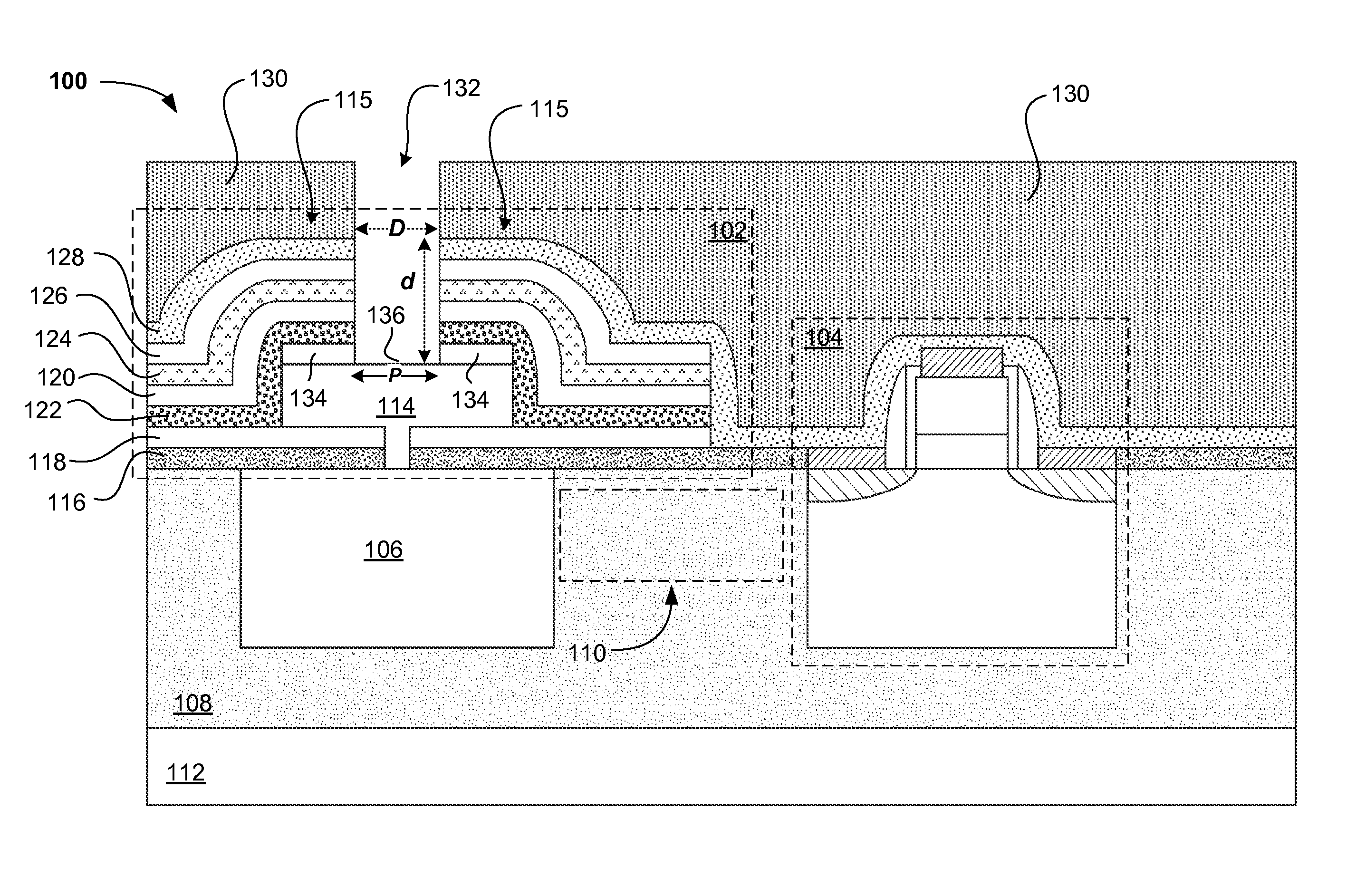
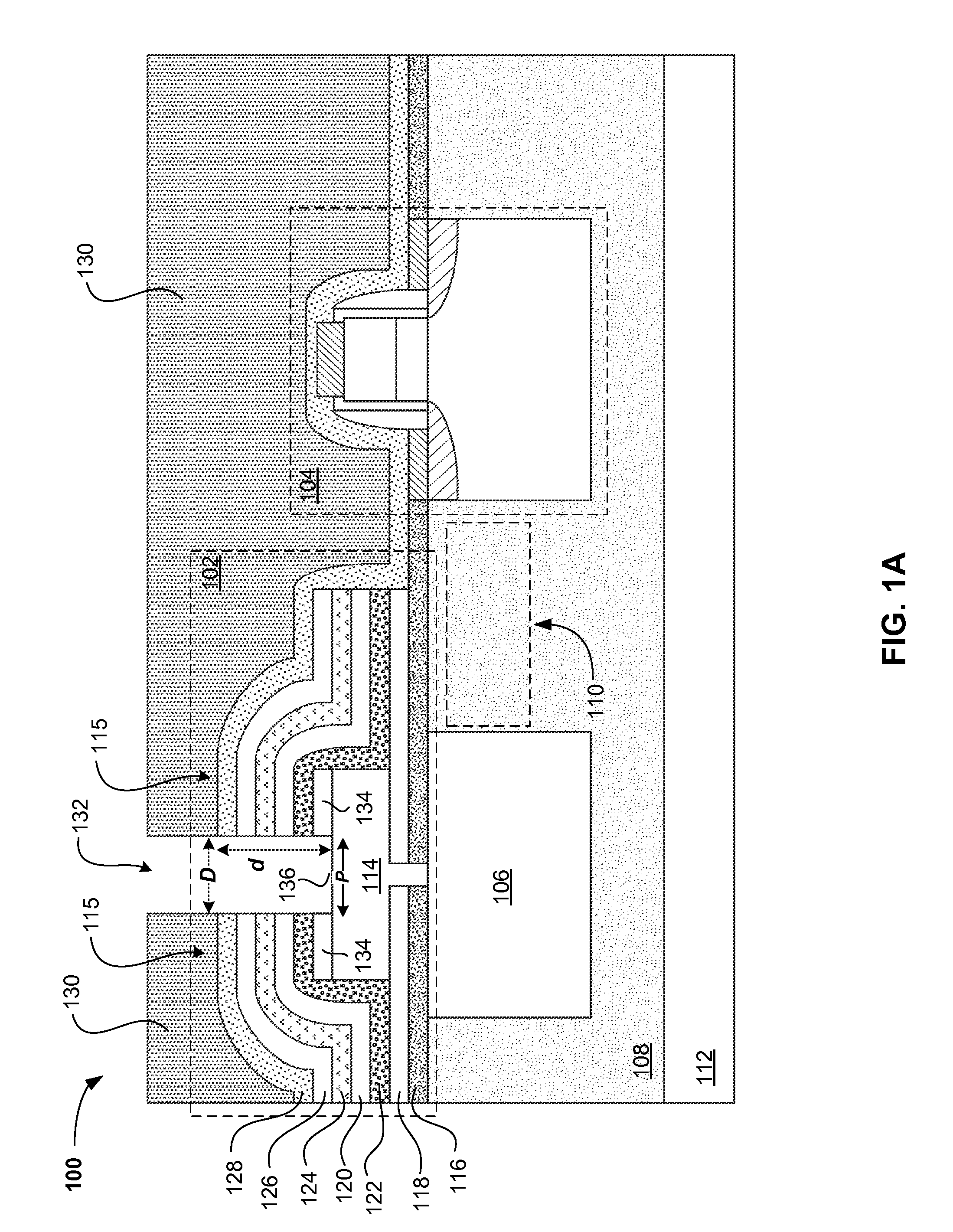
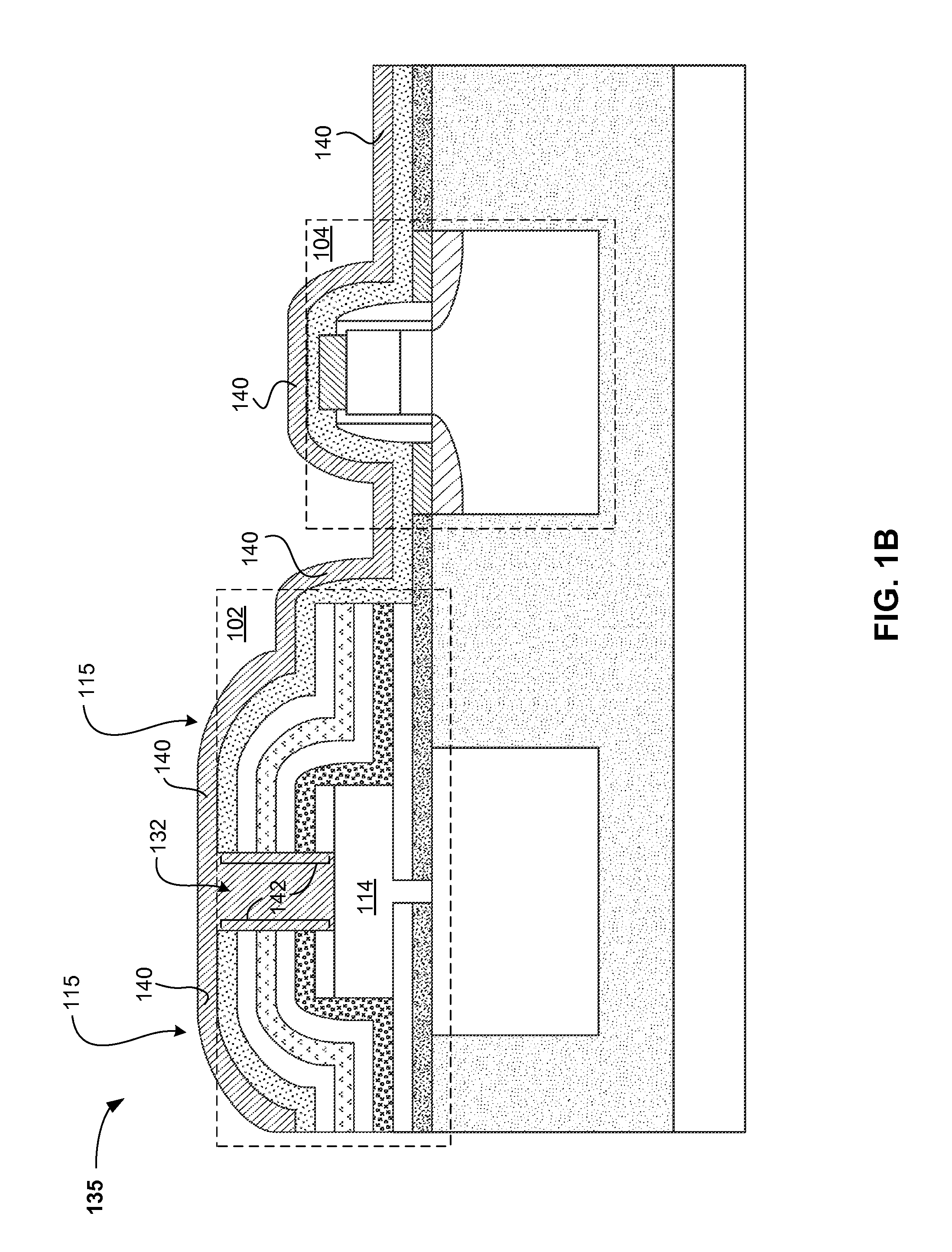
[0014]The following structure and processes provide exemplary embodiments of a CMOS integrated nanophotonics device that includes, for example, both a photonic device such as a Germanium (GE) photodetector and a CMOS device such as an FET transistor. Within the CMOS integrated nanophotonic circuits, crystalline materials such as germanium or III-V compounds may be utilized as an active element of the photodetector component based on their high quantum efficiency. Using a liquid phase epitaxy technique, films (e.g., Germanium) can be deposited at low temperatures in an amorphous state, and subsequently crystallized thermally. During the crystallization process, the Germanium material forming the photodetector active region may be encapsulated, using a film stack, in order to prevent crystalline defects and contamination as a result of outdiffusion. To establish an electrical contact with the Germanium active region, contact integration occurs via the film stack. Electrical contact wi...


PUM


Abstract

A method of forming an integrated photonic semiconductor structure having a photodetector device and a CMOS device may include depositing a dielectric stack over the photodetector device such that the dielectric stack encapsulates the photodetector. An opening is etched into the dielectric stack down to an upper surface of a region of an active area of the photodetector. A first metal layer is deposited directly onto the upper surface of the region of the active area via the opening such that the first metal layer may cover the region of the active area. Within the same mask level, a plurality of contacts including a second metal layer are located on the first metal layer and on the CMOS device. The first metal layer isolates the active area from the occurrence of metal intermixing between the second metal layer and the active area of the photodetector.

Description

BACKGROUND[0001]a. Field of the Invention[0002]The present invention generally relates to semiconductor devices, and particularly to integrated photonic semiconductor devices.[0003]b. Background of Invention[0004]The use of both photonic devices in high-speed switching and transceiver devices in data communications are but a few examples that highlight the advantages of processing both optical and electrical signals within a single integrated device. For example, an integrated photonic device may include both photodetector and CMOS type devices that may be fabricated on a single silicon substrate. However, during the fabrication process, certain processes, while benefiting or being necessary for the formation and / or operation of one type of device (e.g., CMOS FET), may be detrimental to the formation and / or operation of the other type of device (e.g., Photodetector).[0005]One such fabrication process may, for example, include the formation of contacts in integrated photonic devices....

Claims


Application Information

Patent Timeline
Patent Type & Authority Patents(United States)
IPC IPC(8): H01L51/50H01L35/34H01L21/00
CPCH01L35/34G02B6/42H01L51/50H01L31/022408Y02E10/50H01L31/103H01L27/1443H01L27/146H01L31/1808H10N10/01H10K50/00
Inventor ASSEFA, SOLOMONGAMBINO, JEFFREY P.SHANK, STEVEN M.
Owner GLOBALFOUNDRIES US INC
Why Eureka
Try Eureka