Gallium nitride devices having low ohmic contact resistance

a technology of gallium nitride and semiconductors, applied in the direction of semiconductor devices, basic electric elements, electrical equipment, etc., can solve the problems of compromising the carrier concentration and mobility of electrons, high ohmic contact resistance (>0.2 ohm mm), and reducing the yield of source/drain contact spacing of =2 um, so as to achieve the effect of low ohmic contact resistance, and high electron mobility transistor transistor

Active Publication Date: 2014-07-08
RAYTHEON CO
View PDF7 Cites 15 Cited by
  • Summary
  • Abstract
  • Description
  • Claims
  • Application Information

AI Technical Summary

Benefits of technology

[0009]With such an arrangement, the electron donor layer is disposed between and in direct contact with the outer edges of the two-dimension electron gas region and the ohmic contact material, forming, in effect, what might be considered as a high electron mobility transistor (HEMT). The width of the regions for electron injection from the source ohmic contact material and collection of these injected electrons into, and then through, the two-dimension electron gas region, now is significantly increased resulting in lower contact resistance between the electron donor layer and two dimensional electron gas layer. In effect, the formation of this sideways HEMT increases the concentration of electrons all along the contact between the lower semiconductor layer and the electron donor layer results in lower ohmic contact resistance.

Problems solved by technology

One method used to form ohmic contacts for the first generation devices includes forming a Ti / Al / Barrier / Au with rapid thermal annealing at 850-900 C which generally result in devices having high ohmic contact resistance (>0.2 ohm mm), and lower yields for source / drain contact spacing of <=2 um.
This method suffers from two issues: Firstly, etching and exposure of the two dimensional electron gas (2DEG) on the edges might compromise the carrier concentration and mobility of the electrons in the vicinity of the exposed etched surface.

Method used


Image

  • Gallium nitride devices having low ohmic contact resistance
  • Gallium nitride devices having low ohmic contact resistance
  • Gallium nitride devices having low ohmic contact resistance

Examples


Embodiment Construction

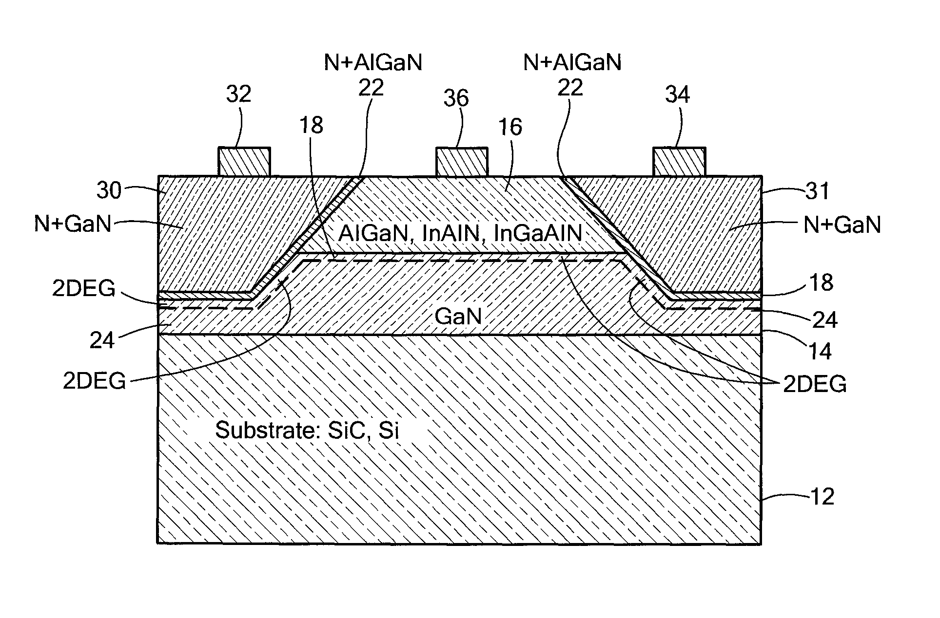
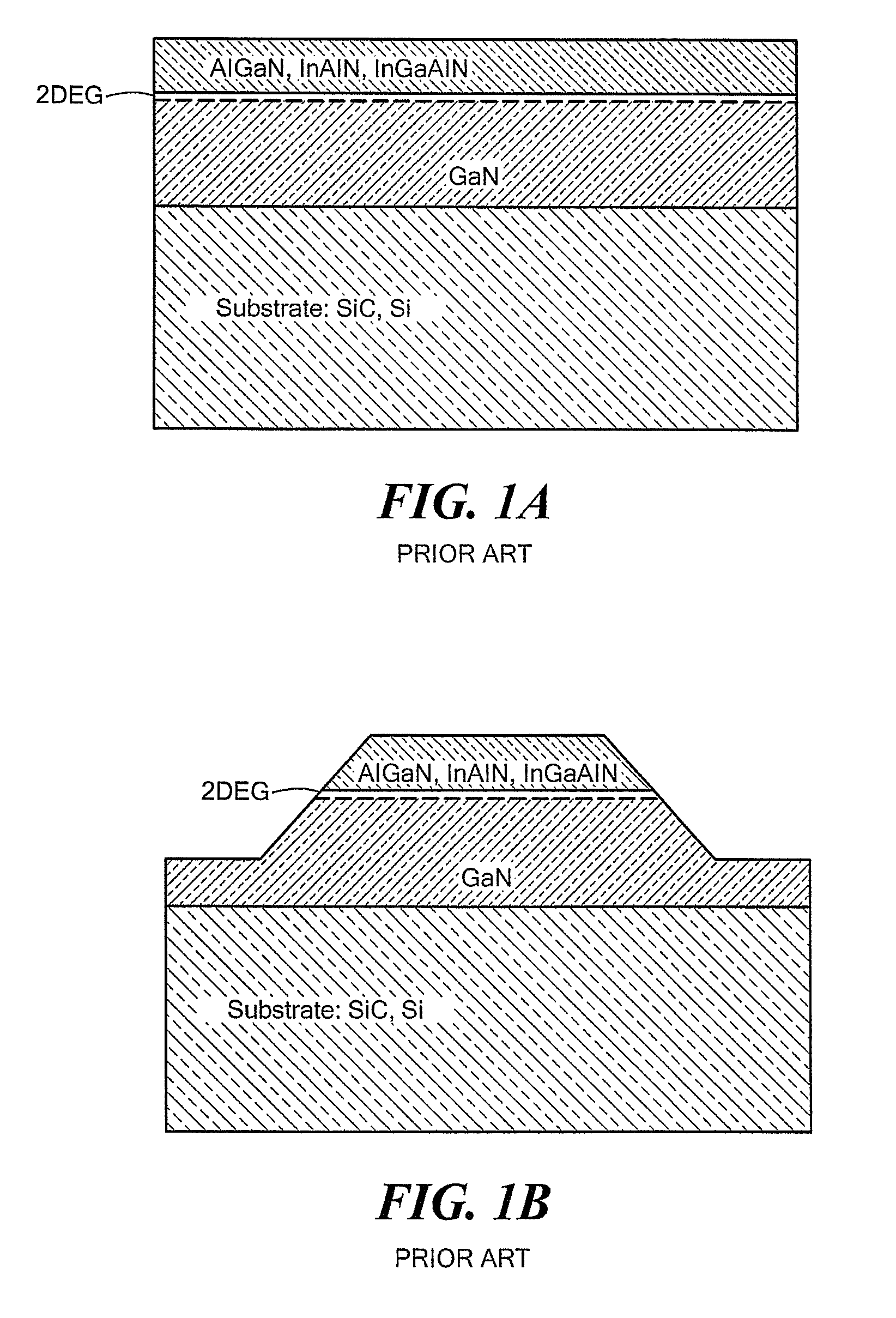
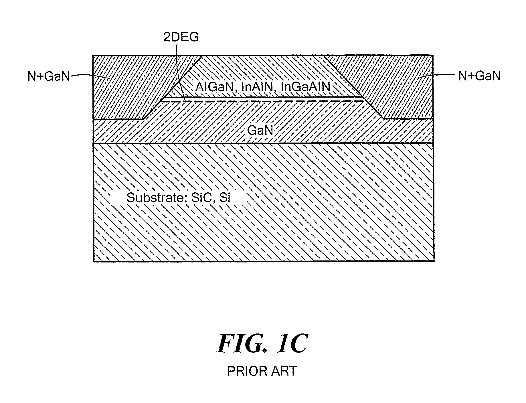
[0021]Referring now to FIG. 2A, a semiconductor structure 10 is shows having: a substrate 12, here a semiconductor substrate of silicon carbide (SiC) or silicon (Si), for example. A lower layer 14 of gallium arsenide (GaN) is formed, by any conventional manner on the substrate 12. An upper layer 16 of aluminum gallium nitride (AlGaN), or indium aluminum nitride (InAlN) or indium gallium aluminum arsenide (InGaAlN) is formed on the lower layer of gallium arsenide (GaN), as shown. Because the upper layer has a higher band gap than the lower layer, a two dimensional electron gas (2DEG) region 18 is formed between the upper and lower layers 14, 16.

[0022]Next, the structure 10 shown in FIG. 2B is masked and dry etched to form a mesa structure 20 shown in FIG. 2B. Here, the structure 10 shown in FIG. 2A is etched to a depth from 300 Angstrom to 1000 Angstrom (preferably 600 Angstrom).

[0023]Next, as shown in FIG. 2C, an additional electron donor N+ layer 22 of AlGaN with Al concentration i...


PUM


Abstract

A semiconductor structure having mesa structure comprising: a lower semiconductor layer; an upper semiconductor layer having a higher band gap than, and in direct contact with, the lower semiconductor layer to form a two-dimension electron gas (2DEG) region between the upper semiconductor layer. The 2DEG region has outer edges terminating at sidewalls of the mesa. An additional electron donor layer has a band gap higher than the band gap of the lower layer disposed on sidewall portions of the mesa structure and on the region of the 2DEG region terminating at sidewalls of the mesa. An ohmic contact material is disposed on the electron donor layer. In effect, a sideway HEMT is formed with the electron donor layer, the 2DEG region and the ohmic contact material increasing the concentration of electrons (i.e., lowering ohmic contact résistance) all along the contact between the lower semiconductor layer and the electron donor layer.

Description

TECHNICAL FIELD[0001]This disclosure relates generally to galliumide (GaN) semiconductor devices and more particularly to gallium nitride (GaN) semiconductor devices having low ohmic contact resistance.BACKGROUND[0002]As is known in the art, second generation GaN HEMI devices (30-300 GHz) must have higher sheet charge in the channel, thinner and higher Al mole fraction AlGaN, InAlN, or InGaAlN Schottky contact layer thicknesses, and lower parasitic ohmic contact resistance (<0.2 ohm mm) than present the present devices.[0003]One method used to form ohmic contacts for the first generation devices includes forming a Ti / Al / Barrier / Au with rapid thermal annealing at 850-900 C which generally result in devices having high ohmic contact resistance (>0.2 ohm mm), and lower yields for source / drain contact spacing of <=2 um.[0004]One method suggested to produce devices having lower ohmic contact resistance is shown in FIGS. 1A-1C. Here, a substrate of, for example, silicon carbide (...

Claims


Application Information

Patent Timeline
Patent Type & Authority Patents(United States)
IPC IPC(8): H01L29/15H01L31/0256
CPCH01L29/66462H01L29/0657H01L29/0843H01L29/2003H01L29/201H01L29/7787H01L29/7789
Inventor TABATABAIE, KAMALHOKE, WILLIAM E.CHUMBES, EDUARDO M.MCCARTHY, KEVIN
Owner RAYTHEON CO
Why Eureka
Try Eureka