
Structure and method to form input/output devices

a technology of input/output devices and structures, applied in the direction of semiconductor devices, electrical equipment, transistors, etc., can solve the problems of inability to reliably operate at voltage, inability to scale, and reduced size of transistors, and achieve the effect of maximizing the commonality of gate dielectric formation processes

Active Publication Date: 2014-09-16
GLOBALFOUNDRIES U S INC
View PDF19 Cites 6 Cited by
  • Summary
  • Abstract
  • Description
  • Claims
  • Application Information

AI Technical Summary

Benefits of technology

This solution provides flexible design of transistors across different size regimes with minimal impact on carrier mobility and BTI parameters, achieving increased breakdown voltage and reduced leakage for I / O transistors while maintaining inversion layer control and scalability.

Problems solved by technology

However, as circuit elements such as transistors are reduced in size, a given design of, for example, a transistor or various functional portions thereof, such as a gate or gate insulator, may or may not be scalable (e.g. proportionally reduced or increased in size from a design of a similar device using a smaller or larger minimum feature size regime.
However, input signals to the integrated circuit and output signals developed in response thereto by the integrated circuit must be interfaced to external circuits and cannot be reliably operated at voltages and currents used by the logic circuitry and memory cells of the integrated circuit in order to achieve, for example, adequate noise immunity and to drive the capacitance and resistance of interconnection circuitry.
Unfortunately, such requirements are very difficult to achieve for different minimum feature size regimes.
For example, use of a dual layer dielectric of a mixture of silicon oxide and silicon nitride (SiON) can be used to achieve a high breakdown voltage in I / O transistors but scaling of the inversion layer (a thin layer at the surface of the conduction channel adjacent the gate structure which is critical to high performance such as on / off resistance ratio, switching threshold, and switching speed / slew rate) is very difficult without compromising leakage and breakdown voltage.

Method used


Image

  • Structure and method to form input/output devices
  • Structure and method to form input/output devices
  • Structure and method to form input/output devices

Examples


Embodiment Construction

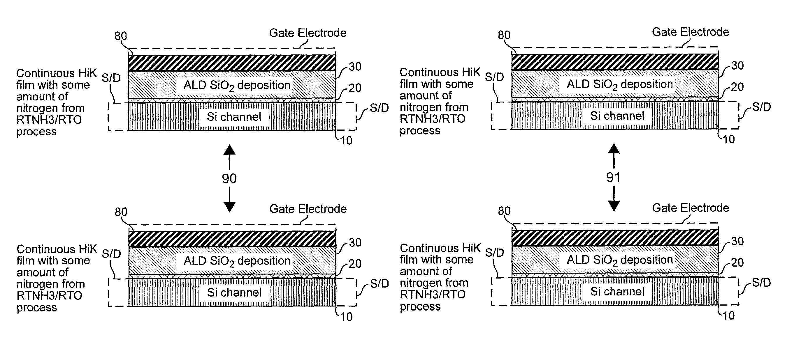
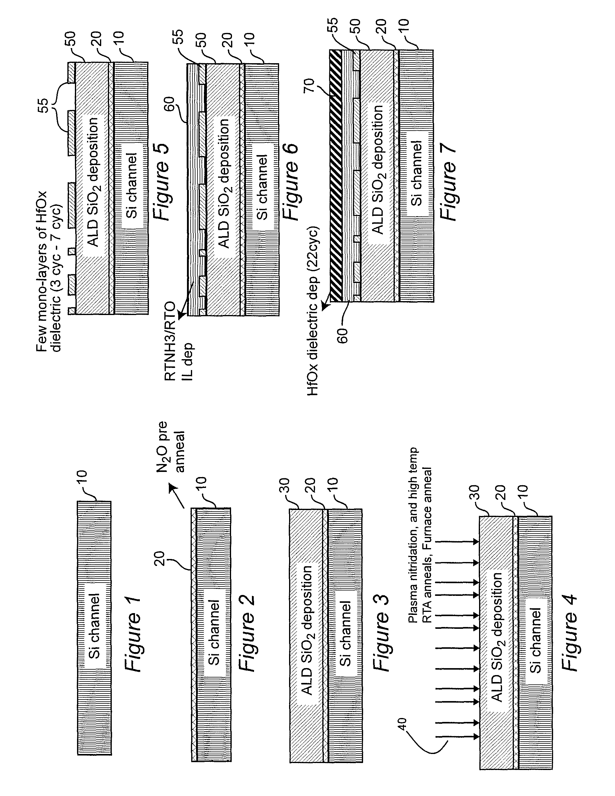
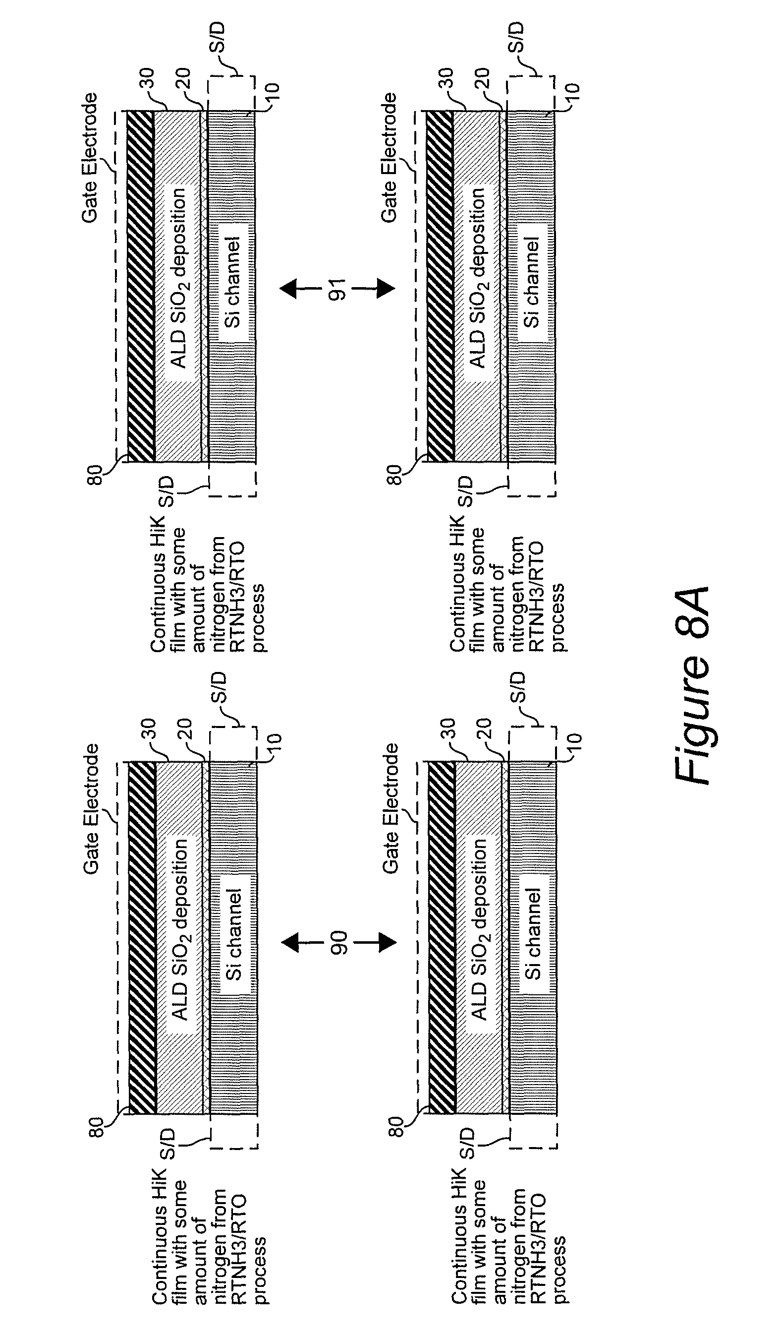
[0014]Referring now to the drawings, and more particularly to FIGS. 1-8A, there is shown a sequence of cross-sectional views of a semiconductor structure illustrating manufacture of an I / O transistor gate structure in accordance with the invention while allowing substantial flexibility of design of logic transistors that are compatible therewith and maximizing the number of processes common to formation of both the logic and I / O transistors on the same chip or wafer. As alluded to above, integrated circuits of current and foreseeable designs provide the highest lithographically feasible levels of integration density for the majority of transistors included therein. These transistors will be predominantly used in logic circuits and memory devices where highest clock rates are highly desirable for highest performance which is achieved through extreme density of formation of such devices so that the interconnection wiring lengths and associated signal propagation times can be minimized...


PUM


Abstract

A limited number of cycles of atomic layer deposition (ALD) of Hi-K material followed by deposition of an interlayer dielectric and application of further Hi-K material and optional but preferred annealing provides increased Hi-K material content and increased breakdown voltage for input / output (I / O) transistors compared with logic transistors formed on the same chip or wafer while providing scalability of the inversion layer of the I / O and logic transistors without significantly compromising performance or bias temperature instability (BTI) parameters.

Description

FIELD OF THE INVENTION[0001]The present invention generally relates to integrated circuits formed at extremely high integration densities and, more particularly, to the formation of input / output (I / O) transistors integrated with such high integration density devices.BACKGROUND OF THE INVENTION[0002]It has long been recognized that numerous benefits may be derived by fabrication of semiconductor integrated circuits at very high integration density in which electronic elements such as transistors are formed with features that are of the minimum lithographically feasible dimensions. For example, close proximity of individual integrated circuit elements reduces signal propagation time (allowing higher clock speeds) and susceptibility to noise while allowing maximum functionality to be developed on a single semiconductor chip of practical dimensions at minimum cost, since the cost of required processes is not affected by the number of circuit elements concurrently formed.[0003]However, a...

Claims


Application Information

Patent Timeline
Patent Type & Authority Patents(United States)
IPC IPC(8): H01L29/78H01L21/314H01L27/088
CPCH01L21/28185H01L21/02181H01L21/28202H01L21/823462H01L29/513H01L29/518
Inventor ANDO, TAKASHIDAI, MINFRANK, MARTIN M.LINDER, BARRY P.SIDDIQUI, SHAHAB
Owner GLOBALFOUNDRIES U S INC
Learn More