Selective deposition of silver for non-volatile memory device fabrication

a technology of non-volatile memory devices and selective deposition, which is applied in the direction of semiconductor devices, basic electric elements, electrical apparatus, etc., can solve the problems of increasing power dissipation, non-scaling of sub-threshold slopes, and reducing device performance, so as to achieve a broader range of applicability

Active Publication Date: 2014-09-23
CROSSBAR INC
View PDF54 Cites 4 Cited by
  • Summary
  • Abstract
  • Description
  • Claims
  • Application Information

AI Technical Summary

Benefits of technology

The present invention provides a method for depositing silver material to create a resistive switching device. This method avoids contamination from a metal etch process and allows for easy scaling of the device. In summary, the invention provides a way to deposit silver in a selective and efficient way.

Problems solved by technology

However, as field effect transistors (FET) approach sizes less than 100 nm, problems such as the short channel effect degrade device performance.
Moreover, such sub 100 nm device sizes can lead to sub-threshold slope non-scaling and increase in power dissipation.
These devices often require new materials and device structures to couple with silicon-based devices to form a memory cell, which lack one or more key attributes.
For example, Fe-RAM and MRAM devices have fast switching characteristics and good programming endurance, but their fabrication is not CMOS compatible and size is usually large.
Switching a PCRAM device requires large amounts of power.
Organic RAM or ORAM is incompatible with large volume silicon-based fabrication and device reliability is usually poor.

Method used


Image

  • Selective deposition of silver for non-volatile memory device fabrication
  • Selective deposition of silver for non-volatile memory device fabrication
  • Selective deposition of silver for non-volatile memory device fabrication

Examples


Embodiment Construction

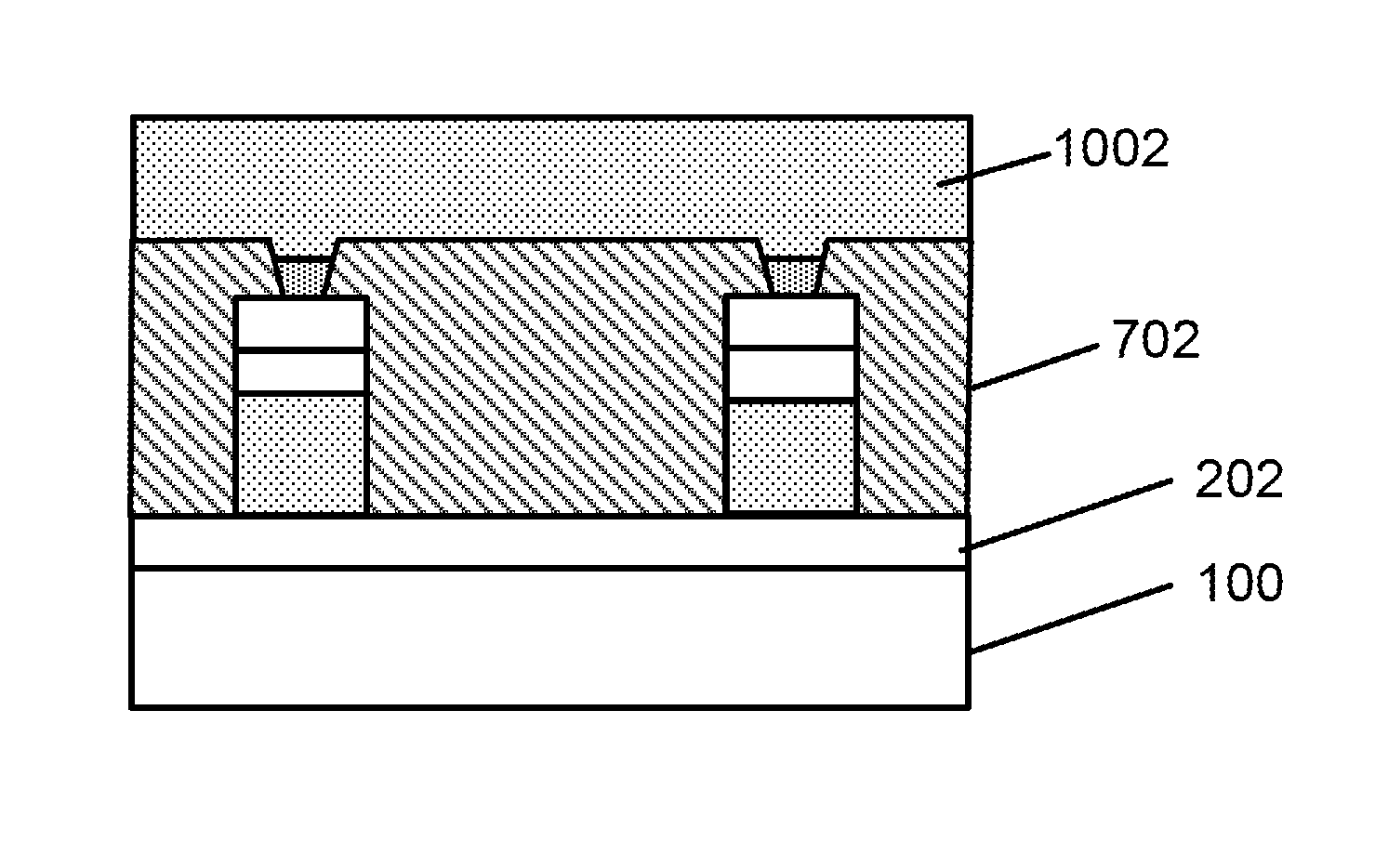
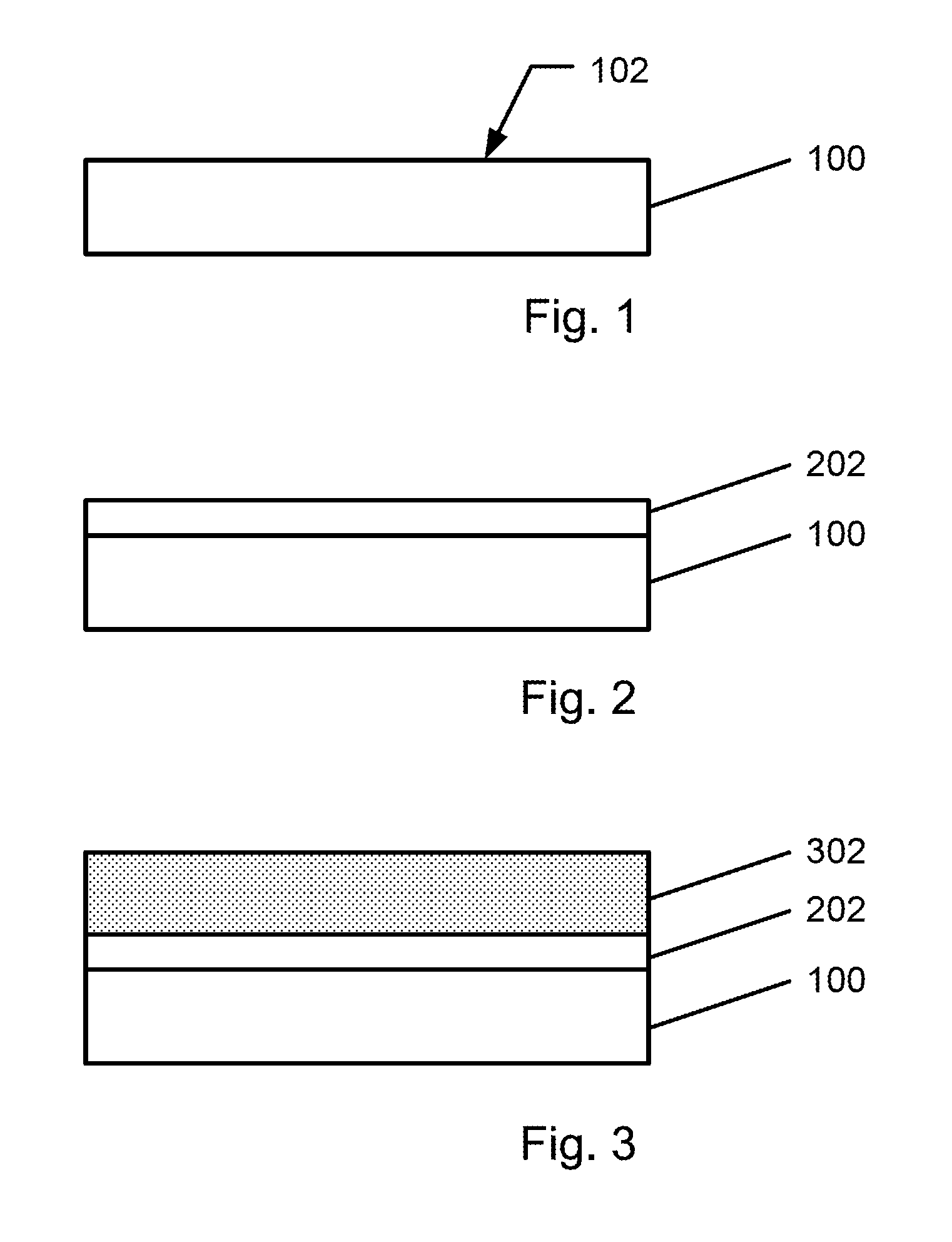
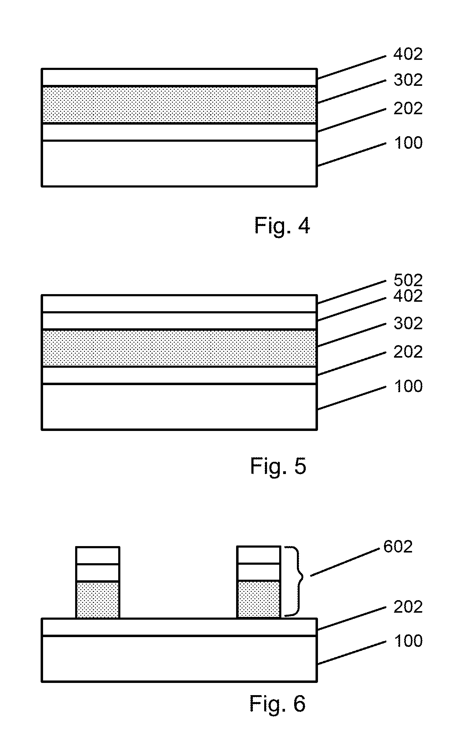
[0011]The present invention is generally related to resistive switching devices. More particularly, embodiments according to the present invention provide a method and a structure for forming a resistive switching device. The present invention can be applied to non-volatile memory devices but it should be recognized that the present invention can have a much broader range of applicability

[0012]In resistive switching using amorphous intrinsic silicon as the switching material, a metal material is usually used as at last one of the electrodes. The metal material forms a metal region in the amorphous intrinsic silicon material in the “on” state. In the “off” state, there is an absence or reduction of metal in the amorphous silicon. The resistance of the amorphous intrinsic silicon material is caused to change depending on a voltage applied to the electrodes. Silver is a material of choice as it has a suitable diffusion characteristic in the amorphous intrinsic silicon material. However...


PUM


Abstract

A method of forming a non-volatile memory device includes providing a semiconductor substrate having a surface region, thereafter forming a first dielectric layer overlying, thereafter forming a first wiring material, thereafter forming amorphous silicon layer, and patterning and etching these layers to form first structures extending in a first direction and having a switching element. Thereafter, a method may include depositing a second dielectric layer overlying the first structures and having a dielectric surface region, forming an opening region in the second dielectric material to exposing part of the switching element, and depositing a silver material in the opening region, but not on the dielectric surface region.

Description

CROSS-REFERENCE TO RELATED APPLICATIONS[0001]The present invention is a non-provisional application of U.S. App. No. 61 / 387,963, filed Sep. 29, 2010. The provisional application is incorporated herein by reference, for all purposes.BACKGROUND[0002]The present invention is generally related to resistive switching devices. More particularly, embodiments according to the present invention provide a method and a structure for forming a resistive switching device. The present invention can be applied to non-volatile memory devices but it should be recognized that the present invention can have a much broader range of applicability.[0003]The success of semiconductor devices has been mainly driven by an intensive transistor down-scaling process. However, as field effect transistors (FET) approach sizes less than 100 nm, problems such as the short channel effect degrade device performance. Moreover, such sub 100 nm device sizes can lead to sub-threshold slope non-scaling and increase in pow...

Claims


Application Information

Patent Timeline
IPC IPC(8): H01L21/20
CPCH01L27/2463H01L45/06H01L45/14H01L27/2436H01L45/085H01L45/148H01L21/76879H01L45/1233H01L45/1675H01L45/00H01L45/16H10B63/80H10N70/245H10N70/826H10N70/884H10N70/011H10N70/063H10B63/30H10N70/231H10N70/881
Inventor HAROLD, SCOTT, BRAD
Owner CROSSBAR INC
Why Eureka
Try Eureka