Two-dimensional touch panel

a touch panel and two-dimensional technology, applied in the field of two-dimensional (2d) touch panels, can solve the problems of cost scaling with the number of signal processing lines required, and achieve the effect of simple and reliable multi-touch sensors and better position resolution

Active Publication Date: 2014-09-23
ATMEL CORP
View PDF31 Cites 22 Cited by
  • Summary
  • Abstract
  • Description
  • Claims
  • Application Information

AI Technical Summary

Benefits of technology

[0020]A simple and reliable multi-touch sensor is thus provided in which the signal processing is based on successive definition of regions or sub-blocks in the touch panel in which signals are excluded in subsequent touch identification steps. This approach can be thought of as an adaptation of the adjacent key suppression (AKS) method of U.S. Pat. No. 6,993,607 [reference 4]. AKS was originally developed for scanning an entire touch panel surface in each data acquisition cycle. The current method differs from conventional AKS in that AKS is applied, not once for the whole key array, but iteratively to sub-blocks of the touch panel, to filter out some keys, i.e. those adjacent to an identified touch location, at each processing stage. The purpose of this localised form of AKS is to exclude keys adjacent to a touch already identified from the search for further valid touches. This is a reliable and simple processing approach which deals with both dimensions, i.e. x and y, together. Specifically, processing according to the invention avoids carrying out the complex signal processing methods of U.S. Pat. No. 5,825,352, which effectively amount to providing a curve fitting analysis to identify both maxima and minima. In particular, identification of minima is not a feature of the present invention, whereas in U.S. Pat. No. 5,825,352 it is an essential prerequisite to resolve multiple touches. Moreover, processing according to the invention avoids having to process data from each of two dimensions separately.
[0024]In the best mode of the invention, the touch location in each region is determined by applying interpolation between the capacitance signal values of at least some of the sensing elements in that region. This allows for a better position resolution in the output than is possible from the sensing elements alone. As a result, a relatively coarse grid of sensing elements is capable of delivering position resolution on a finer scale than the scale of the grid. A simple and reliable multi-touch sensor is thus provided which can be implemented with a relatively low number of sensing elements. Consequently, the capacitance measurement circuit need only comprise a relatively low number of sensing channels.

Problems solved by technology

However, for mass-production devices, cost scales with the number of signal processing lines required, i.e. the number of lines in the capacitance measuring circuitry, ADC, and digital signal processor.

Method used


Image

  • Two-dimensional touch panel
  • Two-dimensional touch panel
  • Two-dimensional touch panel

Examples


first embodiment

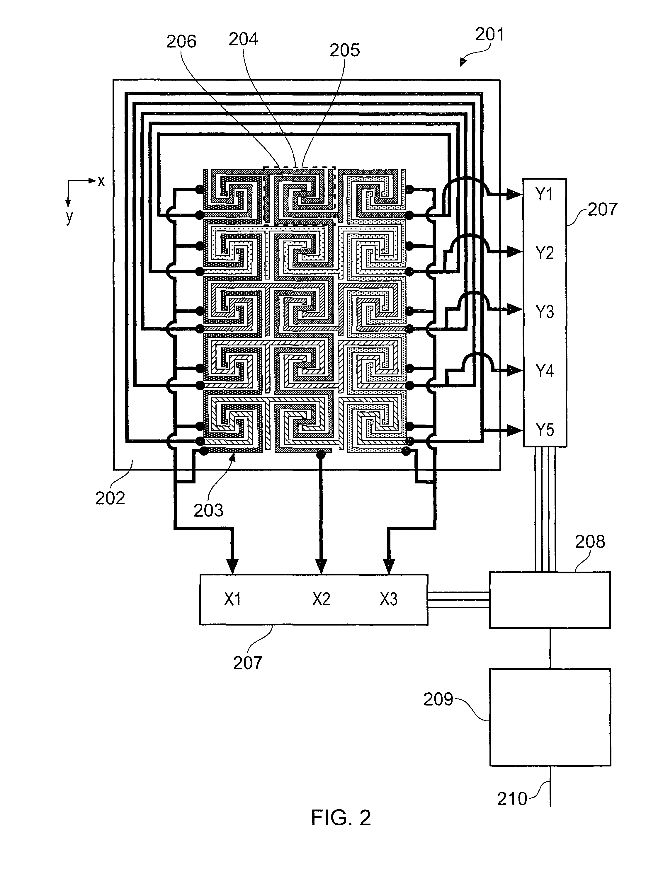
[0047]FIG. 2 schematically shows in plan view a 2D touch-sensitive capacitive position sensor 201 according to the invention. The 2D touch-sensitive capacitive position sensor will be used to describe how the algorithm shown in FIG. 3 is used to compute the position of multiple objects adjacent to the position sensor.

[0048]The 2D touch-sensitive capacitive position sensor 201 is operable to determine the position of objects along a first (x) and a second (y) direction, the orientation of which are shown towards the top left of the drawing. The sensor 201 comprises a substrate 202 having sensing electrodes 203 arranged thereon. The sensing electrodes 203 define a sensing area within which the position of an object (e.g. a finger or stylus) to the sensor may be determined. The substrate 202 is of a transparent plastic material and the electrodes are formed from a transparent film of Indium Tin Oxide (ITO) deposited on the substrate 202 using conventional techniques. Thus the sensing a...

second embodiment

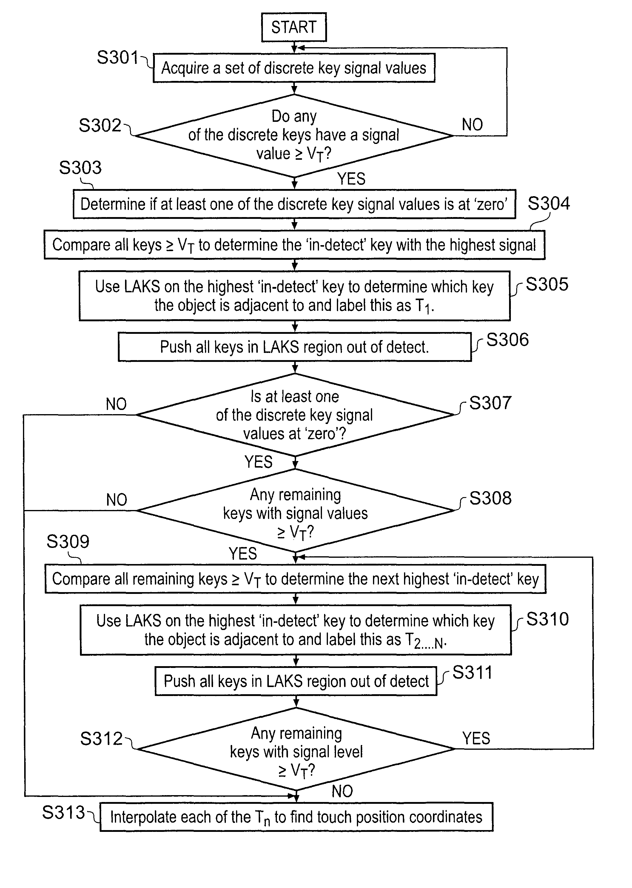
[0115]FIG. 7 is a flow diagram showing steps of the signal processing method embodied in hardware, firmware or software in the host controller 615. FIGS. 8A to 8E show the 4×6 array of touch buttons in the touch panel of the second embodiment in sequence at various points in the processing for the example set of touch inputs.

[0116]FIG. 8A shows a 4×6 grid with the raw data values of the signals acquired in a single acquisition in Step S701 of FIG. 7. Each of the grid squares represents one of the discrete keys of the capacitive position sensor 601. Two simultaneous finger touches are present at the positions indicated by the dashed lines. The raw data values are stated in arbitrary units. There is one finger touch near the top left of the panel and another finger touch near the bottom right of the panel.

[0117]FIG. 8B shows as shaded panels the positions of the five keys that have returned signals above the threshold, i.e. the in-detect keys. Each of the discrete keys is denoted by K...


PUM


Abstract

A capacitive touch panel is provided capable of detecting multiple simultaneous touches. The touch panel delivers sets of capacitance signal values to a processor which computes the coordinates of single or multiple touch locations on the touch panel. The processing of each set is performed by (i) identifying the sensing element having the largest capacitance signal value; (ii) defining a region around that sensing element; and (iii) repeating the process iteratively, wherein each subsequent identifying step excludes signals that lie in previously defined regions. A multi-touch sensor is thus provided in which the signal processing is based on successive definition of regions or sub-blocks in the touch: panel. The touch location in each region can be determined more accurately by then applying interpolation between the adjacent signal values. This allows for position resolution at a finer scale than that defined by the touch panel's electrode patterning.

Description

RELATED APPLICATION[0001]This application is a U.S. National Stage Filing under 35 U.S.C. 371 from International Patent Application Serial No. PCT / GB2008 / 002328, filed Jul. 7, 2008, and published on Jan. 15, 2009 as WO 2009 / 007704 A1, which claims the benefit of U.S. Provisional Application Ser. No. 60 / 949,376, filed on Jul. 12, 2007, the content of which are incorporated herein by reference in their entirety.BACKGROUND OF THE INVENTION[0002]The invention relates to a two-dimensional (2D) touch panel, more especially a touch panel that operates with capacitive touch sensing.[0003]2D touch panels based on capacitive sensing are in widespread use in a variety of applications. Typically, the 2D touch panels are actuated by a finger, either in direct contact, or through proximity (i.e. without contact). For example, they are used as touchpads of laptop computers, in control panels of domestic appliances such as microwave ovens and cooktops, and as overlays to displays on hand held devic...

Claims


Application Information

Patent Timeline
Patent Type & Authority Patents(United States)
IPC IPC(8): G06F3/045G06F3/041G06F3/044
CPCG06F3/044G06F3/0416G06F3/04166G06F3/0446G06F3/0448
Inventor SIMMONS, MARTIN JOHNYILMAZ, ESAT
Owner ATMEL CORP
Why Eureka
Try Eureka