Optical coupling structure and optical transreceiver module

a technology of optical coupling and optical transceiver, applied in the field of optical modules, can solve the problems of high cost of components, high cost of assembly work, increased manufacturing cost, etc., and achieve the effects of high transmission efficiency, easy mounting by die bonding or wire bonding, and excellent transmission characteristics

Inactive Publication Date: 2014-12-09
FUJIKURA LTD
View PDF30 Cites 9 Cited by
  • Summary
  • Abstract
  • Description
  • Claims
  • Application Information

AI Technical Summary

Benefits of technology

[0033]According to the optical coupling structure of the aforementioned (1), it is possible to manufacture an optical connection portion at a low cost without using a number of components, and moreover it is possible to transmit optical signals with higher efficiency.
[0034]Since it is possible to mount a semiconductor element with the optical axis thereof perpendicular to a substrate (the vertical direction in the present invention), it is possible to mount the light receiving / emitting portion of the optical semiconductor element facing the opposite side of the mounting face. Thereby, mounting by die bonding or wire bonding becomes easy. Moreover, it is possible to connect the wiring in the shortest line length, which is important for transmission characteristics, and excellent transmission characteristics are obtained with preventing noise. Further, it becomes easy to perform appearance inspection of the bonding and thus easy to find poor connections.

Problems solved by technology

For that reason, the cost of components, and the cost of the work related to assembly are high, becoming the principal cause of cost increases.
As a result, there is the problem of the manufacturing cost increasing.
As a result, the problem arises of noise easily containing.
Moreover, since it is difficult to perform appearance inspection of the optical semiconductor element that is flip-chip bonded after mounting, it is difficult to discover poor connections thereof.
As a result, there is the problem of the manufacturing cost increasing.
For that reason, in the case of for example, both optical axes being mutually perpendicular or the like, when attempting to convert an optical path, the problem arises of this method being inapplicable.
However, in the case of making an optical signal incident on the light receiving element from an optical fiber with a small aperture angle, or making it incident on an optical fiber from a light emitting element, when the coupling efficiency is low, there is the problem of ensuring the reliability of transmission of the optical signal being difficult.
For that reason, when forming a step in a substrate, since it is necessary to design and manufacture the position and shape of the resin interface in accordance with the shape and size of the step, the manufacturing cost rises.
However, forming the resin so that the interface of the resins is positioned just at the position of that intersection point is not easy.

Method used


Image

  • Optical coupling structure and optical transreceiver module
  • Optical coupling structure and optical transreceiver module
  • Optical coupling structure and optical transreceiver module

Examples


example 1

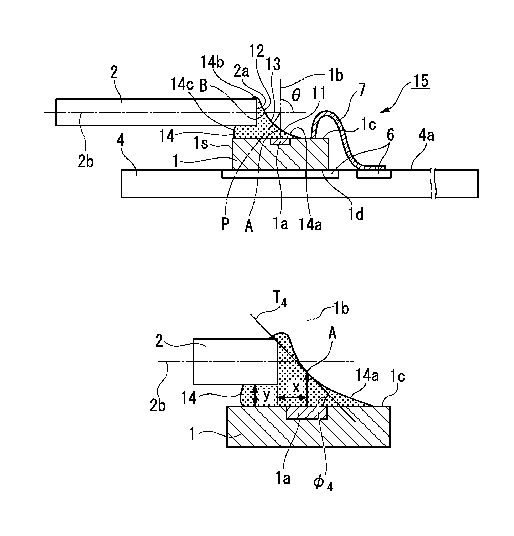
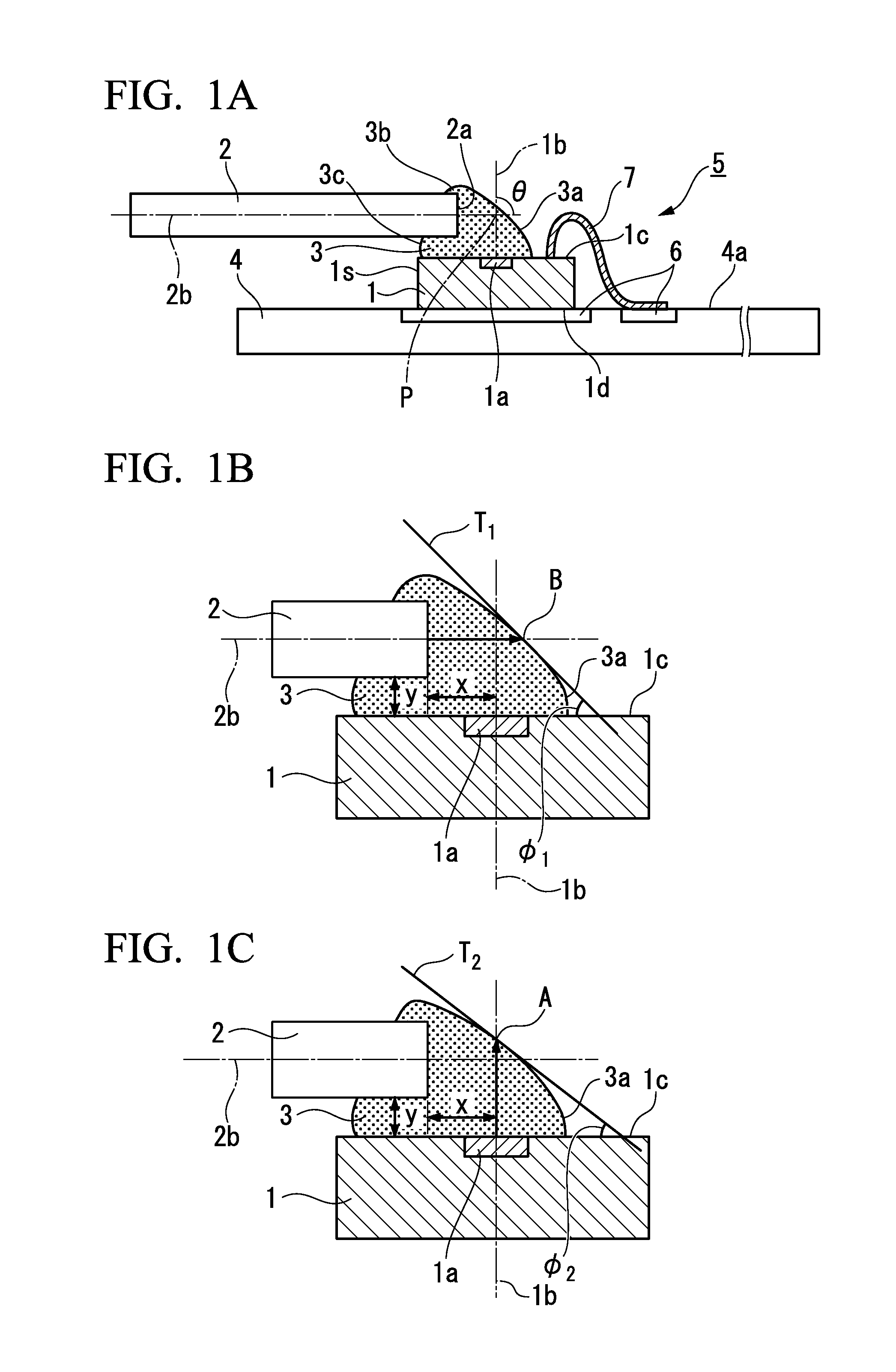
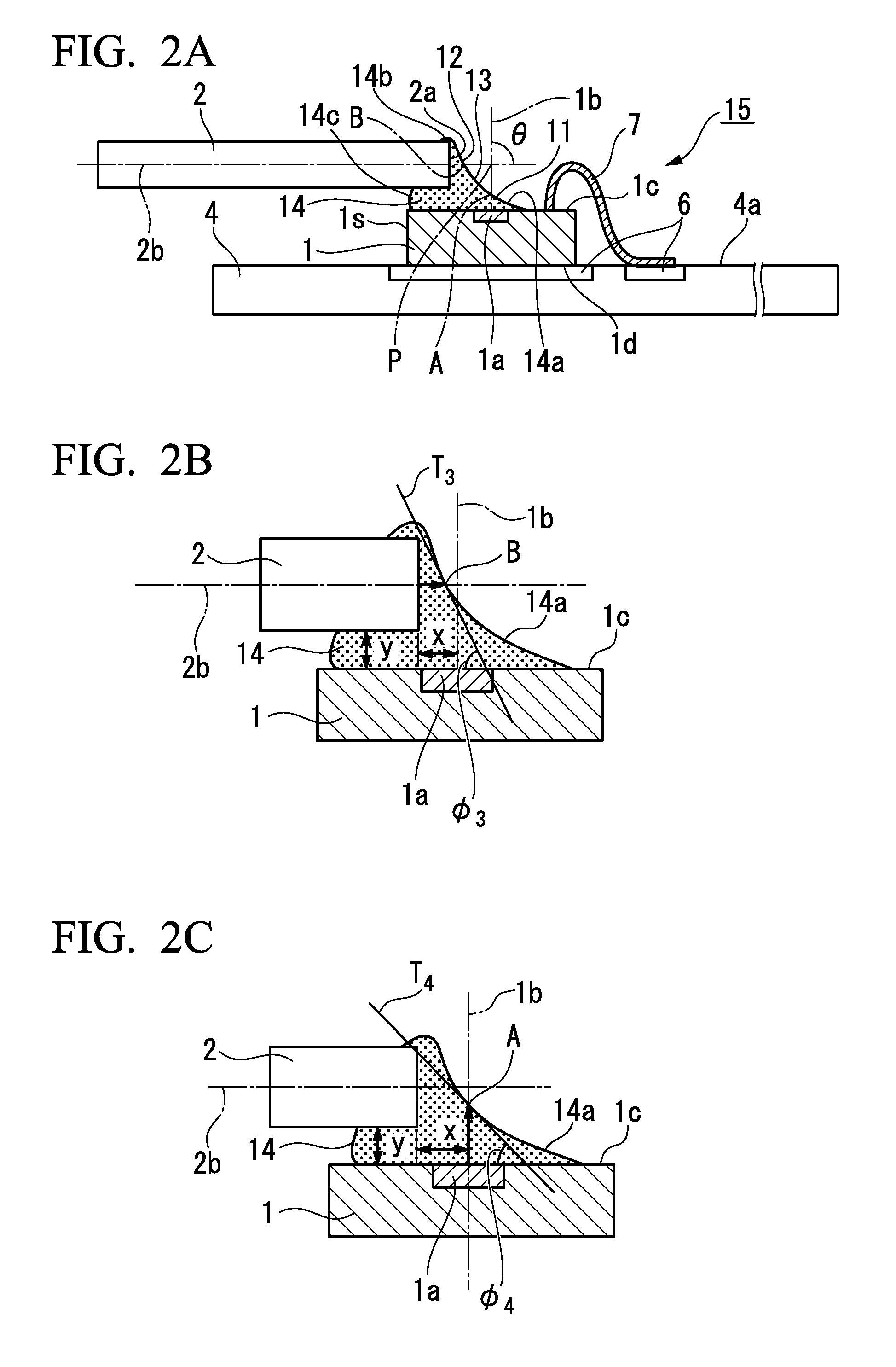
[0178]As shown in FIGS. 1A to 4, as the optical transmission path 2, a silica based multi-mode optical fiber with a cladding diameter of 125 μm and a core diameter of 50 μm was prepared. For the optical semiconductor element 1, a PD (aperture diameter of the light receiving portion being 80 μm) was used as the light receiving element, a VCSEL (aperture diameter of the light emitting portion being 12 μm) was used as the light emitting element, a UV-curable resin (acrylic resin) is used for the transparent resin 31, a glass-epoxy substrate was used as the substrate 4, and a gold wire was used for the wire interconnect 7. After applying 2 nl (nanoliters) of the transparent resin 31 on the light receiving / emitting portion 1a (the light receiving portion of the PD or the light emitting portion of the VCSEL) of the optical semiconductor element 1, the distal end of the optical fiber was inserted into the transparent resin, and the optical fiber was pulled up a distance of 40 μm obliquely ...

example 2

[0185]Optical coupling portions were fabricated with the period of time from pulling up the optical diver to UV irradiation being constant, and the shape of each obtained optical coupling portion was observed. Table 3 shows the case of the period of time from pulling up the optical fiber to UV radiation being 3 seconds, and Table 4 shows the case of the time from pulling up the optical fiber to UV radiation being 2 minutes.

[0186]

TABLE 3Period of time from pulling up optical fiber to UV radiation: 3 secondsSample NameABCDEFGHIJKViscosity (Pa · s)0.020.10.71.53.25.51521263550Range of OpticalViscosity is tooNo contact with wireCoupling Portionlow, so resindoes notremain onelementShape of Optical—ConcaveConvex shapeCoupling Portionshape

[0187]

TABLE 4Period of time from pulling up optical fiber to UV radiation: 2 minutesSample NameABCDEFGHIJKViscosity (Pa · s)0.020.10.71.53.25.51521263550Range of OpticalViscosity is tooContactNo contact with wireCoupling Portionlow, so resinwith wiredoes ...


PUM


Abstract

Provided is an optical coupling structure including an optical semiconductor element including a light receiving / emitting portion, an optical transmission path having an optical axis that intersects the optical axis of the optical semiconductor element at a predetermined angle, and an optical coupling portion configured to convert the optical path between the optical semiconductor element and the optical transmission path and optically couple them. The optical coupling portion is made of a resin that is transparent with respect to a transmitted light, the resin adhering to both at least a portion of the light receiving / emitting portion and at least a portion of the end portion of the optical transmission path, and the optical semiconductor element and the optical transmission path are bonded to each other with the resin itself that constitutes the optical coupling portion.

Description

CROSS REFERENCE TO RELATED APPLICATIONS[0001]This application is a continuation application based on a PCT Patent Application No. PCT / JP2011 / 050076, filed Jan. 6, 2011, whose priority is claimed on Japanese Patent Application No. 2010-001100 filed Jan. 6, 2010, the entire content of which are hereby incorporated by reference.BACKGROUND OF THE INVENTION[0002]1. Field of the Invention[0003]The present invention relates to an optical module that is used in optical communication technology, optical transmission technology, and optical information recording technology, and in particular relates to an optical coupling structure that optically couples an optical semiconductor element and an optical transmission path in an optical module.[0004]2. Description of the Related Art[0005]An optical module is equipped with an optical semiconductor element that is mounted on a substrate, and an optical transmission path that is arranged so that the optical axis is parallel with the substrate.[0006]...

Claims


Application Information

Patent Timeline
Patent Type & Authority Patents(United States)
IPC IPC(8): H01S5/022G02B6/30G02B6/42H01S5/40
CPCH01S5/02284H01S5/02292H01S5/0226H01L2224/45144H01L2224/48091G02B6/4239H01S5/4025G02B6/4214G02B6/422H01S5/02276H01L2224/45147H01L2224/45124H01S5/0236H01S5/02345H01S5/02255H01S5/02251H01L2924/00014
Inventor KIMURA, NAOKITAKIGAHIRA, MASATO
Owner FUJIKURA LTD
Why Eureka
Try Eureka