Supercharge Your Innovation With Domain-Expert AI Agents!

Superior integrity of high-k metal gate stacks by capping STI regions

a technology of capping regions and gate stacks, applied in the direction of basic electric elements, electrical apparatus, semiconductor devices, etc., to achieve superior surface topography in isolation regions, reduce the degree of receding, and improve the effect of efficiency

Active Publication Date: 2014-12-23
GLOBALFOUNDRIES U S INC
View PDF11 Cites 3 Cited by
  • Summary
  • Abstract
  • Description
  • Claims
  • Application Information

AI Technical Summary

Benefits of technology

The present disclosure provides a way to make semiconductor devices more efficiently with better protection for sensitive gate materials. This is done by reducing the amount of material that needs to be removed from the active regions in order to create shallow valleys for isolation. By using a special dielectric layer and resisting multiple cleaning processes, the surface topography of the materials is improved, leading to better performance and fewer failures. This technique also helps conserve the sensitive gate material during subsequent processing, such as the formation of a strain-inducing semiconductor alloy, while also improving overall surface topography.

Problems solved by technology

It has been recognized that, in particular, the recessed configuration of trench isolation regions in close proximity to active regions may significantly contribute to yield losses caused by gate failures or gate deterioration.

Method used


Image

  • Superior integrity of high-k metal gate stacks by capping STI regions
  • Superior integrity of high-k metal gate stacks by capping STI regions
  • Superior integrity of high-k metal gate stacks by capping STI regions

Examples


Embodiment Construction

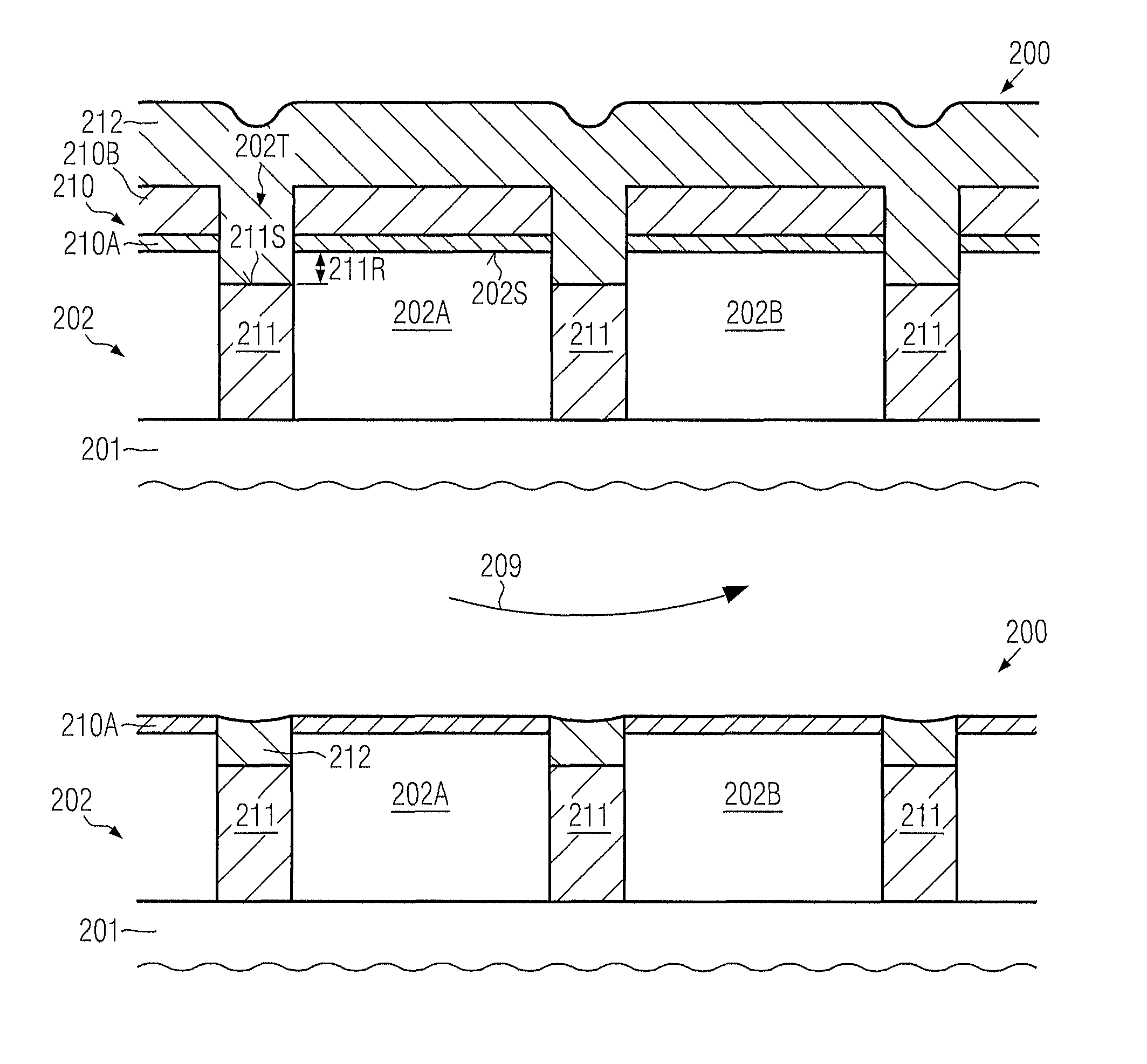
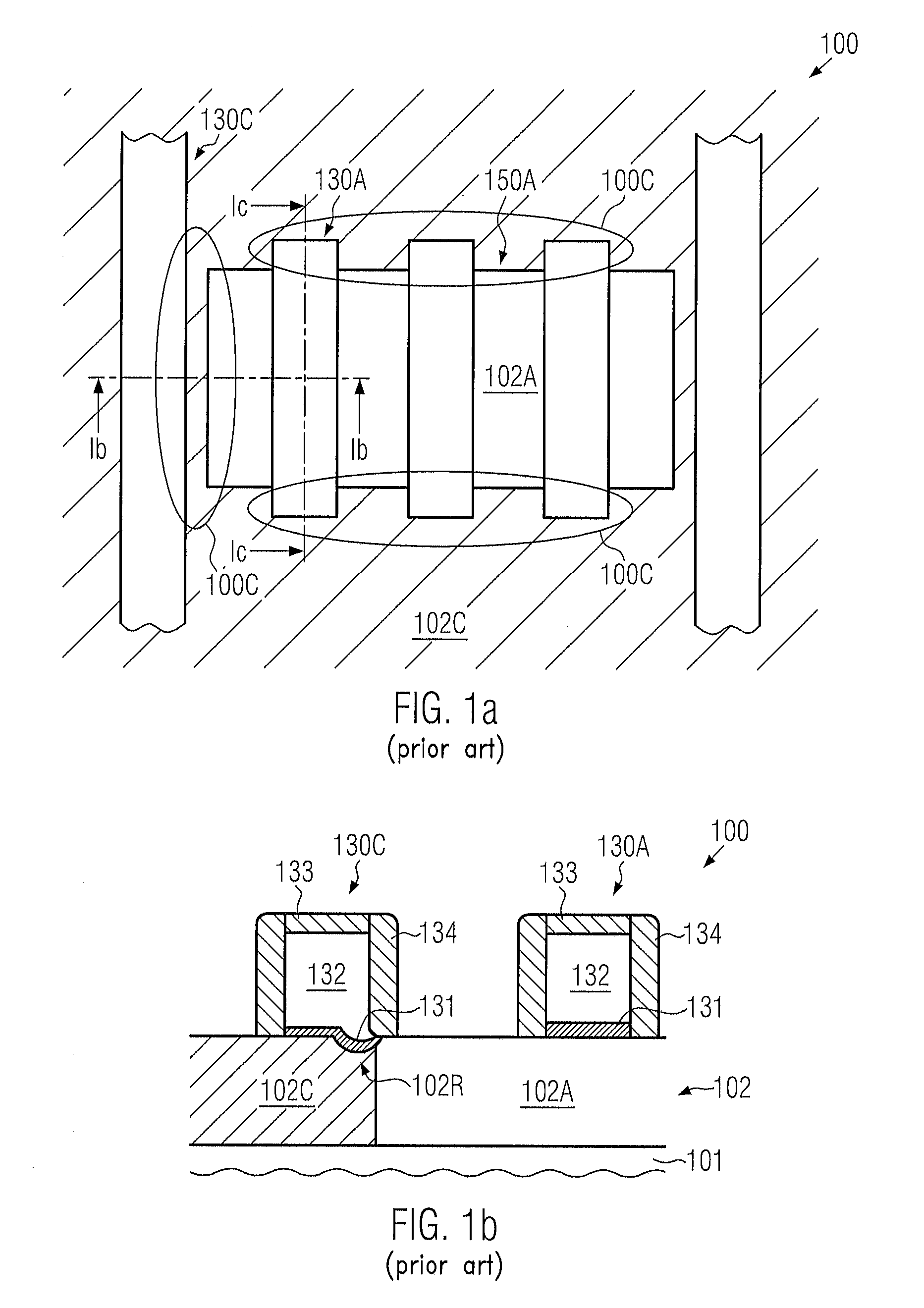
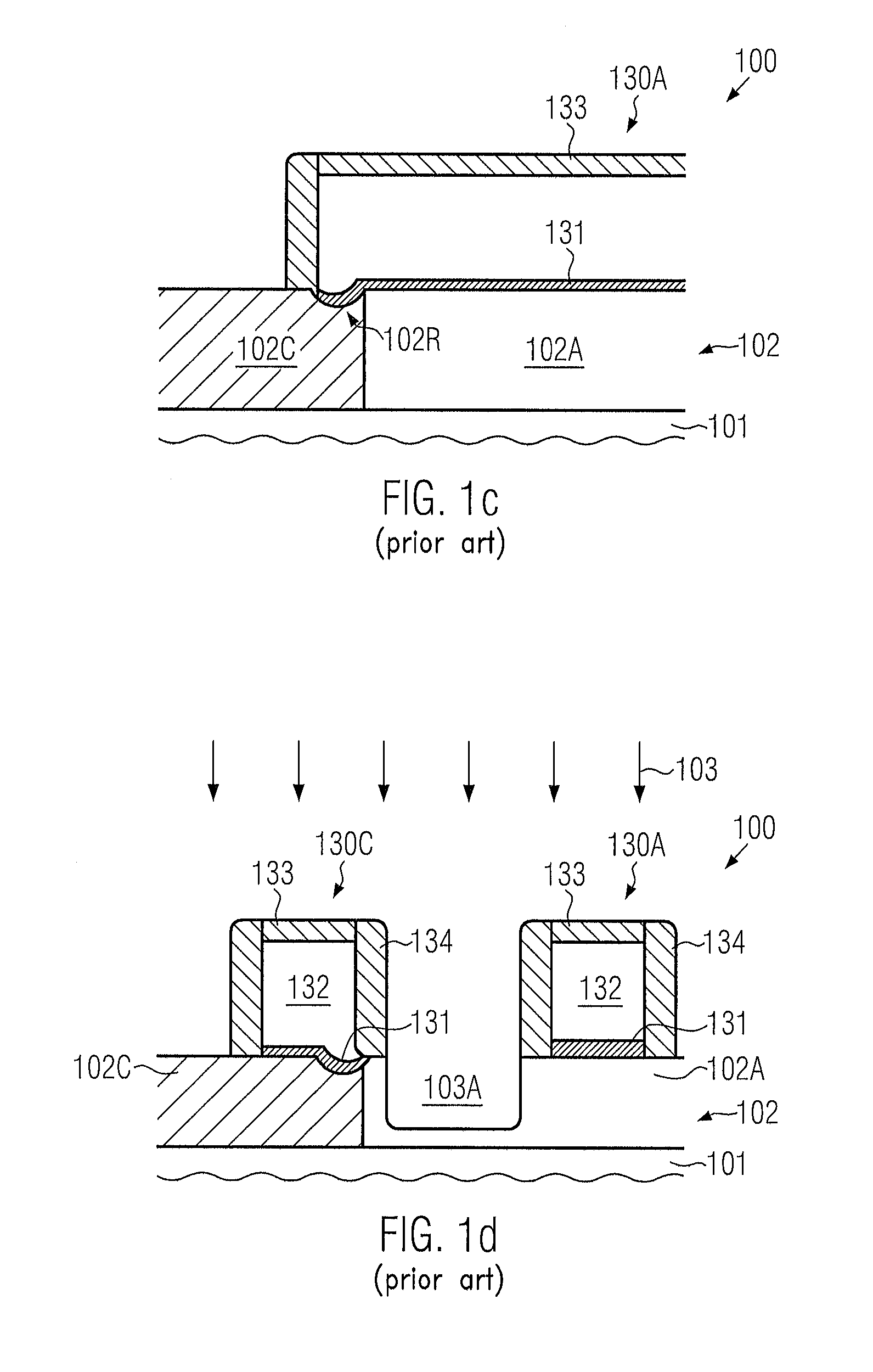
[0034]Various illustrative embodiments of the invention are described below. In the interest of clarity, not all features of an actual implementation are described in this specification. It will of course be appreciated that in the development of any such actual embodiment, numerous implementation-specific decisions must be made to achieve the developers' specific goals, such as compliance with system-related and business-related constraints, which will vary from one implementation to another. Moreover, it will be appreciated that such a development effort might be complex and time-consuming, but would nevertheless be a routine undertaking for those of ordinary skill in the art having the benefit of this disclosure.

[0035]The present subject matter will now be described with reference to the attached figures. Various structures, systems and devices are schematically depicted in the drawings for purposes of explanation only and so as to not obscure the present disclosure with details ...


PUM

PropertyMeasurementUnit
thicknessaaaaaaaaaa
gate lengthaaaaaaaaaa
thicknessaaaaaaaaaa

Abstract

When forming high-k metal gate electrode structures in an early manufacturing stage, integrity of an encapsulation and, thus, integrity of sensitive gate materials may be improved by reducing the surface topography of the isolation regions. To this end, a dielectric cap layer of superior etch resistivity is provided in combination with the conventional silicon dioxide material.

Description

BACKGROUND OF THE INVENTION[0001]1. Field of the Invention[0002]Generally, the present disclosure relates to the fabrication of highly sophisticated integrated circuits including advanced transistor elements that comprise gate structures of increased capacitance including a high-k gate dielectric material.[0003]2. Description of the Related Art[0004]The fabrication of advanced integrated circuits, such as CPUs, storage devices, ASICs (application specific integrated circuits) and the like, requires the formation of a large number of circuit elements on a given chip area according to a specified circuit layout. In a wide variety of integrated circuits, field effect transistors represent one important type of circuit element that substantially determines performance of the integrated circuits. Generally, a plurality of process technologies are currently practiced for forming field effect transistors, wherein, for many types of complex circuitry, CMOS technology is one of the most prom...

Claims


Application Information

Patent Timeline
Patent Type & Authority Patents(United States)
IPC IPC(8): H01L29/51H01L29/78H01L29/10H01L21/8238H01L21/461H01L21/336H01L21/28H01L21/8234H01L21/76H01L21/762H01L29/49
CPCH01L21/823425H01L21/823878H01L29/7848H01L29/513H01L21/823828H01L29/78H01L21/76232H01L29/1054H01L21/28123H01L29/4966H01L21/823481H01L21/823437
Inventor SCHEIPER, THILOBAARS, PETERBEYER, SVEN
Owner GLOBALFOUNDRIES U S INC
Features
  • R&D
  • Intellectual Property
  • Life Sciences
  • Materials
  • Tech Scout
  • Unparalleled Data Quality
  • Higher Quality Content
  • 60% Fewer Hallucinations
Learn More