Wavelength converting devices

a conversion device and wavelength technology, applied in the field of wavelength conversion devices, can solve the problems of difficult to obtain original high oscillation efficiency, deviation of oscillation output of harmonic waves over time, etc., to reduce the reduction of conversion efficiency, improve the connection efficiency, and reduce the deterioration of the domain inverted part.

Active Publication Date: 2014-12-23
NGK INSULATORS LTD
View PDF18 Cites 0 Cited by
  • Summary
  • Abstract
  • Description
  • Claims
  • Application Information

AI Technical Summary

Benefits of technology

[0008]The inventors have tried to optically connect a fiber grating to a solid phase laser oscillator to fabricate an external type resonator and to utilize the resonator for a light source of fundamental wave to oscillate a harmonic wave at a high efficiency. In this case, the fiber grating is used to reduce the deviation of wavelength of the fundamental wave as possible by accurately controlling a width of the wavelength of the fundamental wave. At the same time, it was tried to attain a high efficiency of wavelength conversion by improving the precision of the period of the periodic domain inversion structure. Since the deviation of the wavelength of the fundamental wave is prevented, it should have been prevented the reduction or unstableness of the efficiency of the wavelength conversion due to peak out, even in the case that the precision of production of the period is improved to reduce the width of the phase matching wavelength.
[0011]An object of the present invention is to prevent the reduction of efficiency of conversion due to feedback of the return light and to further improve an output power of a harmonic wave.
[0018]Second, for improving the efficiency of connection to the semiconductor laser functioning as the fundamental wave, the width of the domain inverted part of the wavelength converting device tends to become larger than the thickness. According to the prior art shown in FIG. 3, the domain inversion boundary was inclined toward the longer width direction. It is thus considered that the shift of the time points at which the light pass through the inverted part becomes larger.
[0019]Contrary to this, according to the present invention, when the substrate of the ferroelectric material is viewed in a cross section parallel with a direction of propagation of a fundamental wave and parallel with the normal line of an upper face of the ferroelectric substrate, a vertical domain inversion boundary of the periodic domain inversion structure is inclined with respect to the normal line of the upper face. It is thus possible to reduce the deterioration in the domain inverted part as well as to sufficiently reduce the reduction of conversion efficiency due to the feedback of the return light, so that the output power of the harmonic wave as a whole can be further improved.

Problems solved by technology

However, when it was actually fabricated, it was found that the oscillation output of the harmonic wave may be deviated over time.
However, although it was possible to prevent the reduction of the efficiency of wavelength conversion due to return light, it was proved to be difficult to obtain original high oscillation efficiency.

Method used


Image

  • Wavelength converting devices
  • Wavelength converting devices
  • Wavelength converting devices

Examples


example a1

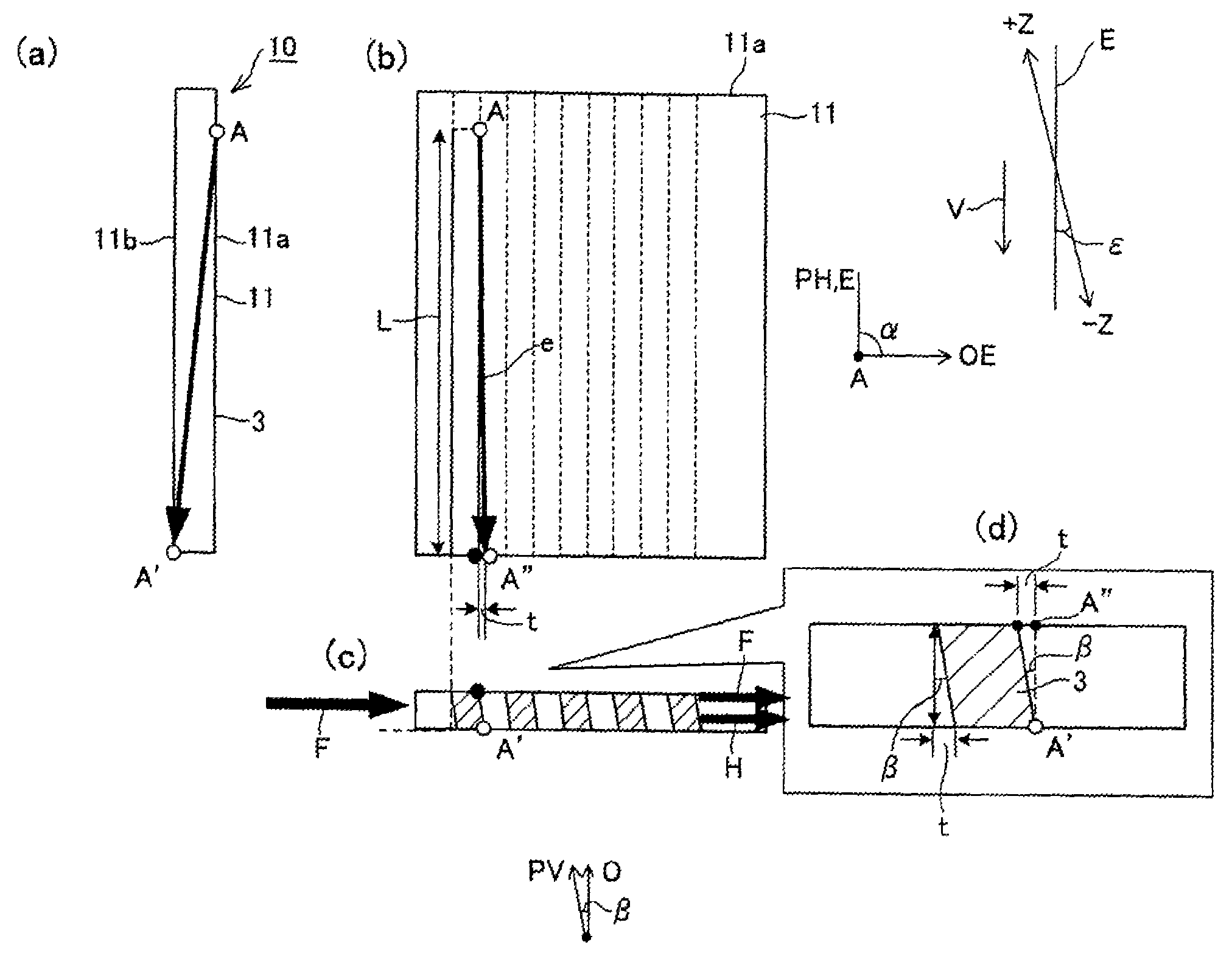
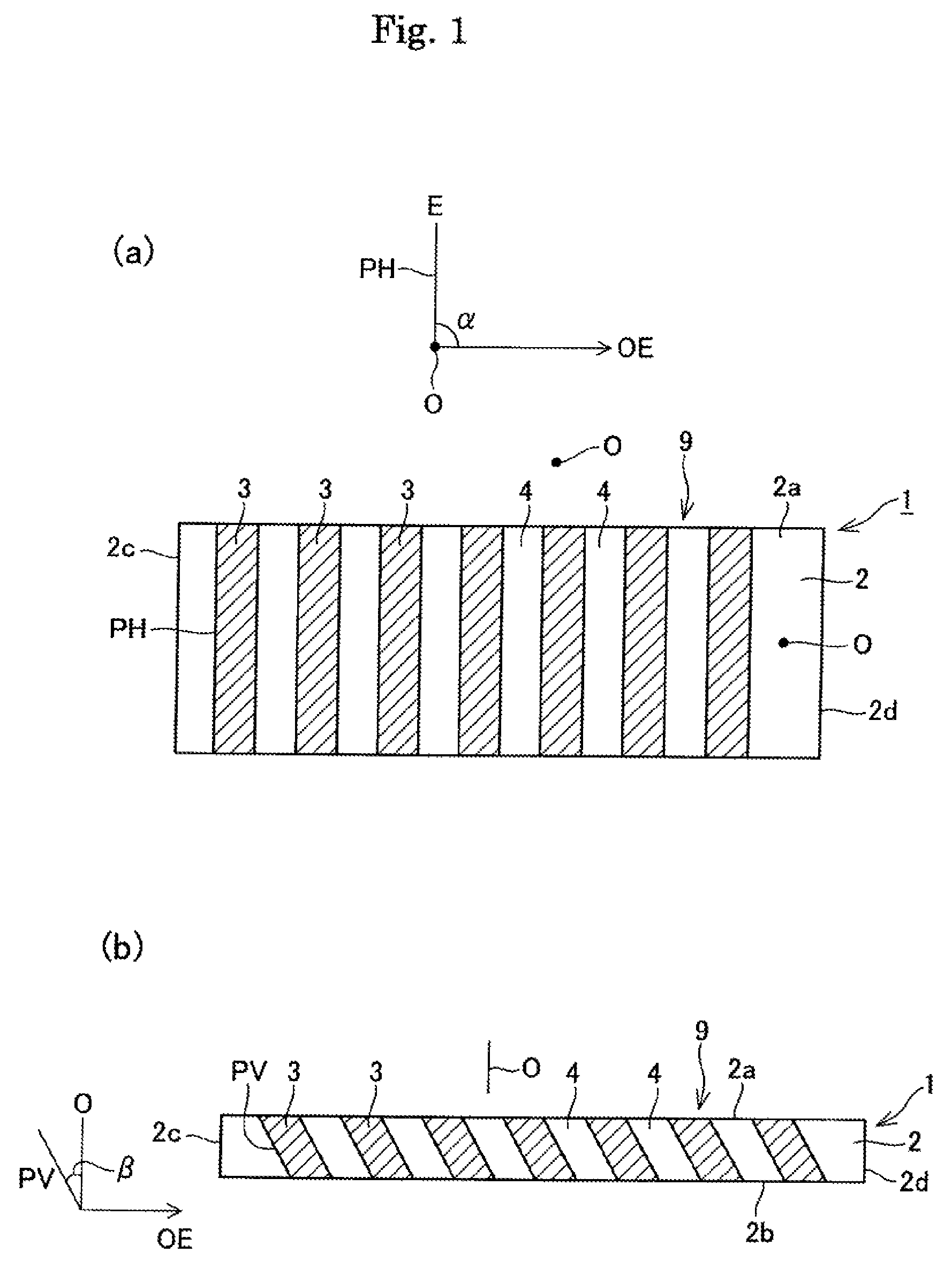
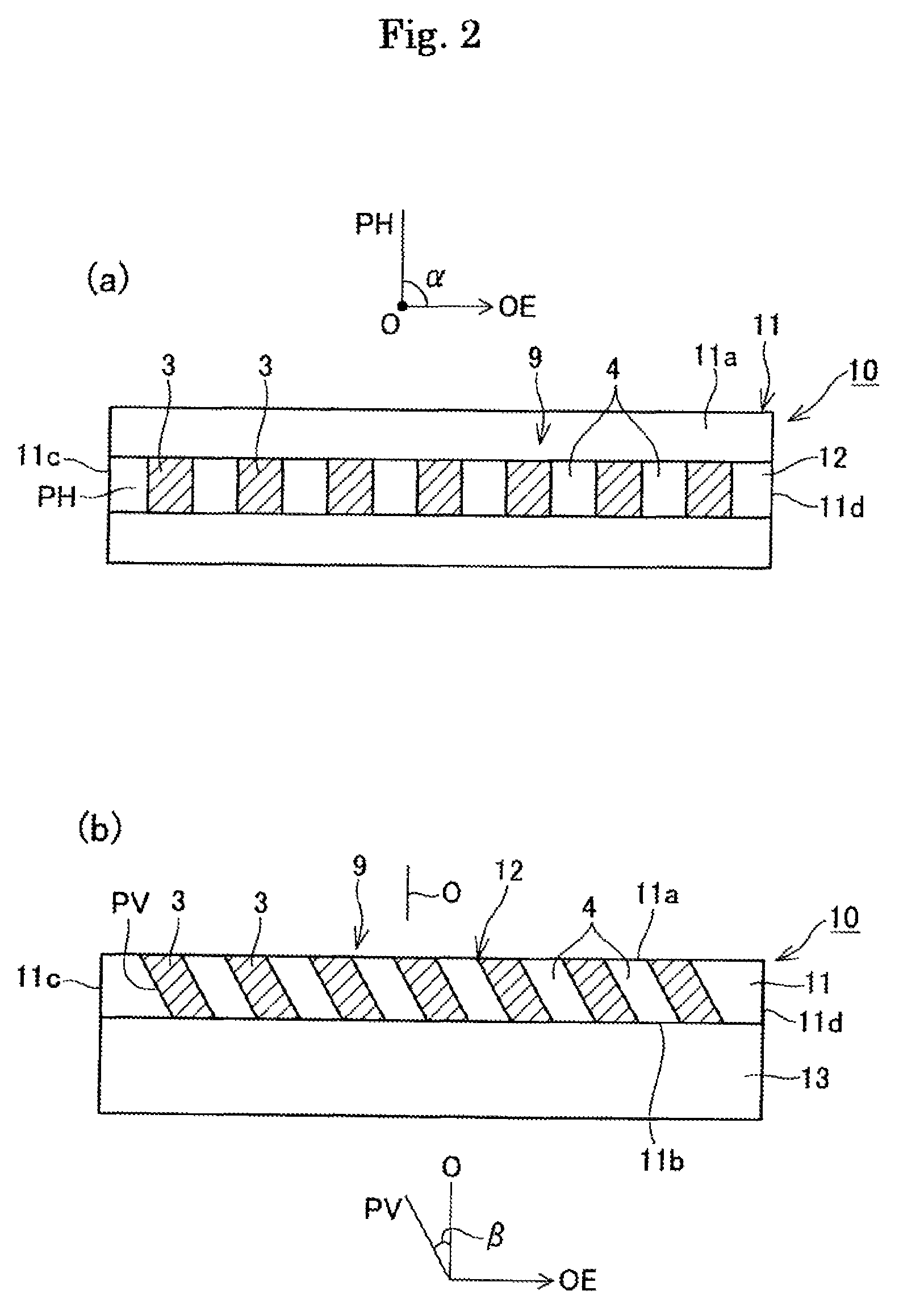
[0091]It was fabricated the wavelength converting device having the shape shown in FIGS. 1 to 8.

[0092]Specifically, a comb like electrode and a counter electrode were formed on a upper face and an uniform electrode is formed on a bottom face of an off-cut Y plate having a thickness of 0.5 mm and of MgO 5% doped lithium niobate. A periodic domain inversion structure having a period of 5.08 μm was formed by voltage application method.

[0093]On the other hand, an adhesive was applied on a substrate of a non-doped lithium niobate and having a thickness of 0.5 mm. Then, it was adhered onto the MgO-doped lithium niobate substrate, and the surface of the MgO-doped lithium niobate substrate was ground and polished to a thickness of 3.5 μm to produce a thin plate.

[0094]Then, a channel type optical waveguide of ridge type was formed on the thin plate by laser ablation process. After forming the optical waveguide, it was formed an over clad of SiO2 and having a thickness of 0.5 g m by sputterin...

examples a2

to A5

[0098]Wavelength converting devices were produced according to the same procedure as the Example A1. However, each parameter was changed as follows.

[0099]

ε:0.1° (Example A2);0.3° (Example A3)1° (Example A4);2° (Example A5)t:0.07 μm (Example A2);0.21 μm (Example A3)0.7 μm (Example A4);1.4 μm (Example A5)β:1.1° (Example A2);3.4° (Example A3)11° (Example A4);22° (Example A5)

[0100]The oscillating output power was measured as the Example A1, and the following SHG output powers were obtained. The wavelength at this time was proved to be 975.9 to 976.4 m. The measurement was performed at room temperature (25° C.). The differences of the wavelengths of the fundamental waves were due to the deviation of thickness of the MgO-doped lithium niobate substrates fabricated for the respective examples. The state of oscillation of the semiconductor laser light was stable and deviation of output power was not observed in each of the examples.

[0101]

Example A2;84mWExample A3;83.5mWExample A4;76mWE...

example b1

[0105]A wavelength converting device was produced according to the same procedure as the Example A1. However, the construction shown in FIG. 9 was applied. The respective parameters were changed as follows.

[0106]

OC: 5°, ε: 0.2°, γ: 0.3°L: 40 μm, β: 5.7°

[0107]The SHG oscillating power was measured according to the same procedure as the Example A1 to prove that the SHG output power was 82.5 mW at the wavelength of the fundamental wave of 976.2 nm. The measurement was performed at room temperature (25° C.). The state of oscillation of the semiconductor laser light was stable and deviation of output power was not observed.


PUM

PropertyMeasurementUnit
inclined angleaaaaaaaaaa
wavelengthaaaaaaaaaa

Abstract

It is provided a wavelength converting device comprising a periodic domain inversion structure for converting a wavelength of a fundamental wave to generate a harmonic wave. The wavelength conversion device includes a ferroelectric substrate and the periodic domain inversion structure formed in the ferroelectric substrate. A vertical domain inversion boundary of the periodic domain inversion structure is inclined with respect to a normal line of an upper face of the ferroelectric substrate, provided that the ferroelectric substrate is viewed in a cross section parallel with a propagating direction of the fundamental wave and parallel with the normal line of the upper face.

Description

TECHNICAL FIELD OF THE INVENTION[0001]The present invention relates to a wavelength conversion device.RELATED ART[0002]Blue light laser has been commercialized using a semiconductor material of GaN series, and already utilized for a light source for a display. Up to now, in a semiconductor laser of GaN series, the oscillating wavelength is made longer so that laser oscillation has been confirmed near green light band. However, the GaN semiconductor laser of GaN series, including the commercialized blue laser, has a problem that its consuming electric power is large.[0003]On the other hand, although a laser utilizing a wavelength converting device requires many number of parts for the fabrication, its consuming electric power is small and quality of beam emitted from its optical waveguide is good. The efficiency of utilization of light is thereby advantageously high even at an optical output same as that used for the semiconductor laser of GaN series. Further, as the wavelength is st...

Claims


Application Information

Patent Timeline
Patent Type & Authority Patents(United States)
IPC IPC(8): G02F1/377G02F1/37G02F1/35
CPCG02F1/37G02F1/3775G02F2001/3548G02F1/3548
Inventor TANI, MINORIASAI, KEIICHIROYAMAGUCHI, SHOICHIRO
Owner NGK INSULATORS LTD
Why Eureka
Try Eureka