Semiconductor device, method for manufacturing the semiconductor device, and method for controlling the semiconductor device

a semiconductor device and semiconductor technology, applied in the direction of semiconductor/solid-state device details, pulse technique, electronic switching, etc., can solve the problems of increasing the total electric loss of the a-npc circuit, increasing the turn-on loss eon of the igbts b>101/b> and b>102/b> constituting the main switch b>100/b>, and reducing the peak of reverse recovery current.

Inactive Publication Date: 2015-01-06
FUJI ELECTRIC CO LTD
View PDF4 Cites 9 Cited by
  • Summary
  • Abstract
  • Description
  • Claims
  • Application Information

AI Technical Summary

Benefits of technology

[0041]According to the aforementioned invention, when the second semiconductor element (RB-IGBT) is brought into reverse recovery, turn-on di / dt of the first semiconductor element (IGBT) whose collector or emitter is connected to the collector or emitter of the second semiconductor element is made smaller than 0.8 kA / μs. Thus, it is possible to suppress the peak of a reverse recovery current and the peak of a jump voltage during the reverse recovery, while it is possible to reduce the reverse recovery loss.
[0042]According to a semiconductor device, a method for manufacturing the semiconductor device and a method for controlling the semiconductor device according to the invention, there is an effect that it is possible to provide a low-loss semiconductor device.

Problems solved by technology

However, in the A-NPC circuit using the RB-IGBTs 131 and 132 as shown in FIG. 33, there is a problem that the total electric loss of the A-NPC circuit increases.
Further, there occurs a problem that the turn-on loss Eon of the IGBTs 101 and 102 constituting the main switch 100 also increases.

Method used


Image

  • Semiconductor device, method for manufacturing the semiconductor device, and method for controlling the semiconductor device
  • Semiconductor device, method for manufacturing the semiconductor device, and method for controlling the semiconductor device
  • Semiconductor device, method for manufacturing the semiconductor device, and method for controlling the semiconductor device

Examples


embodiment 1

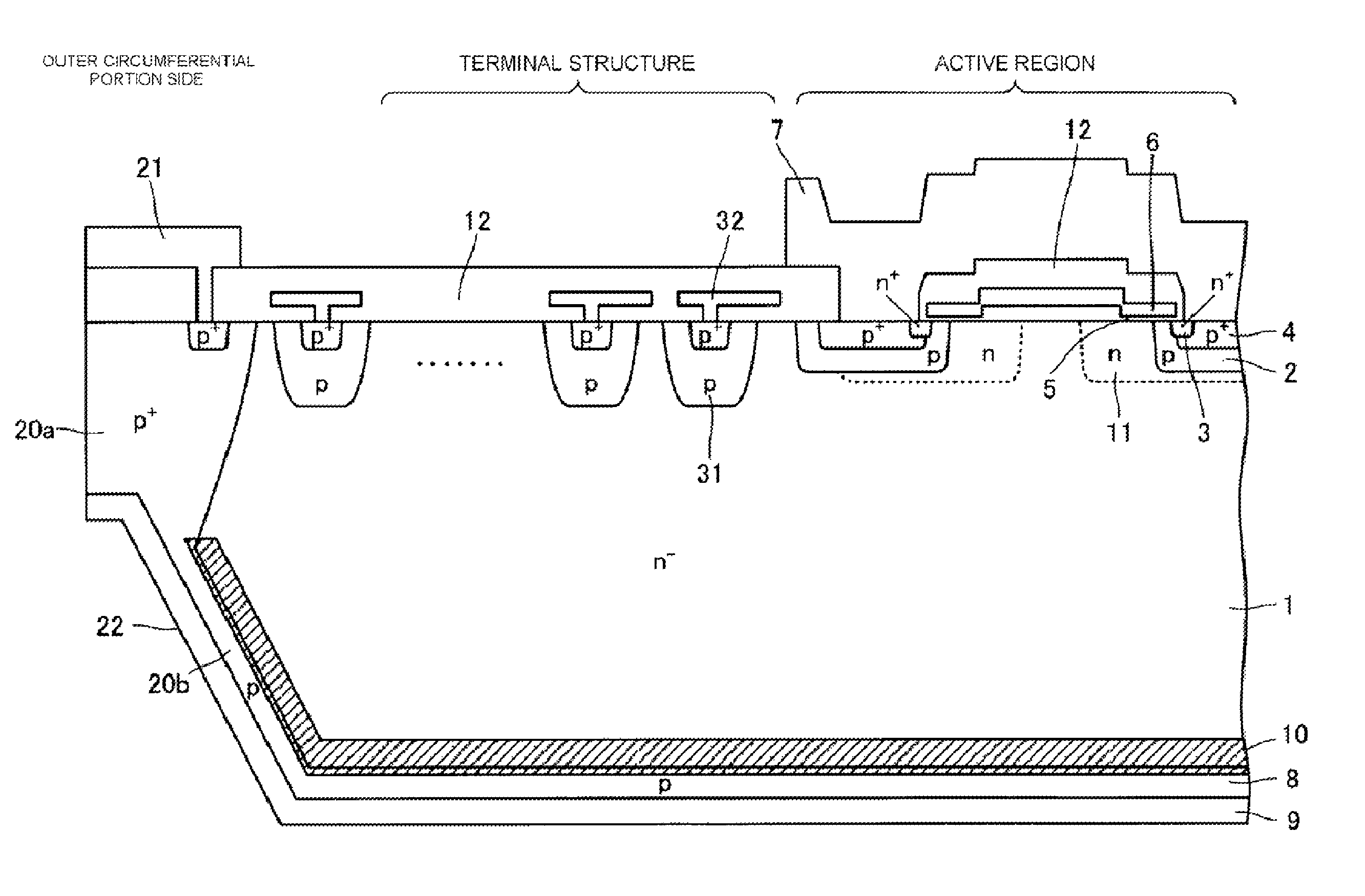
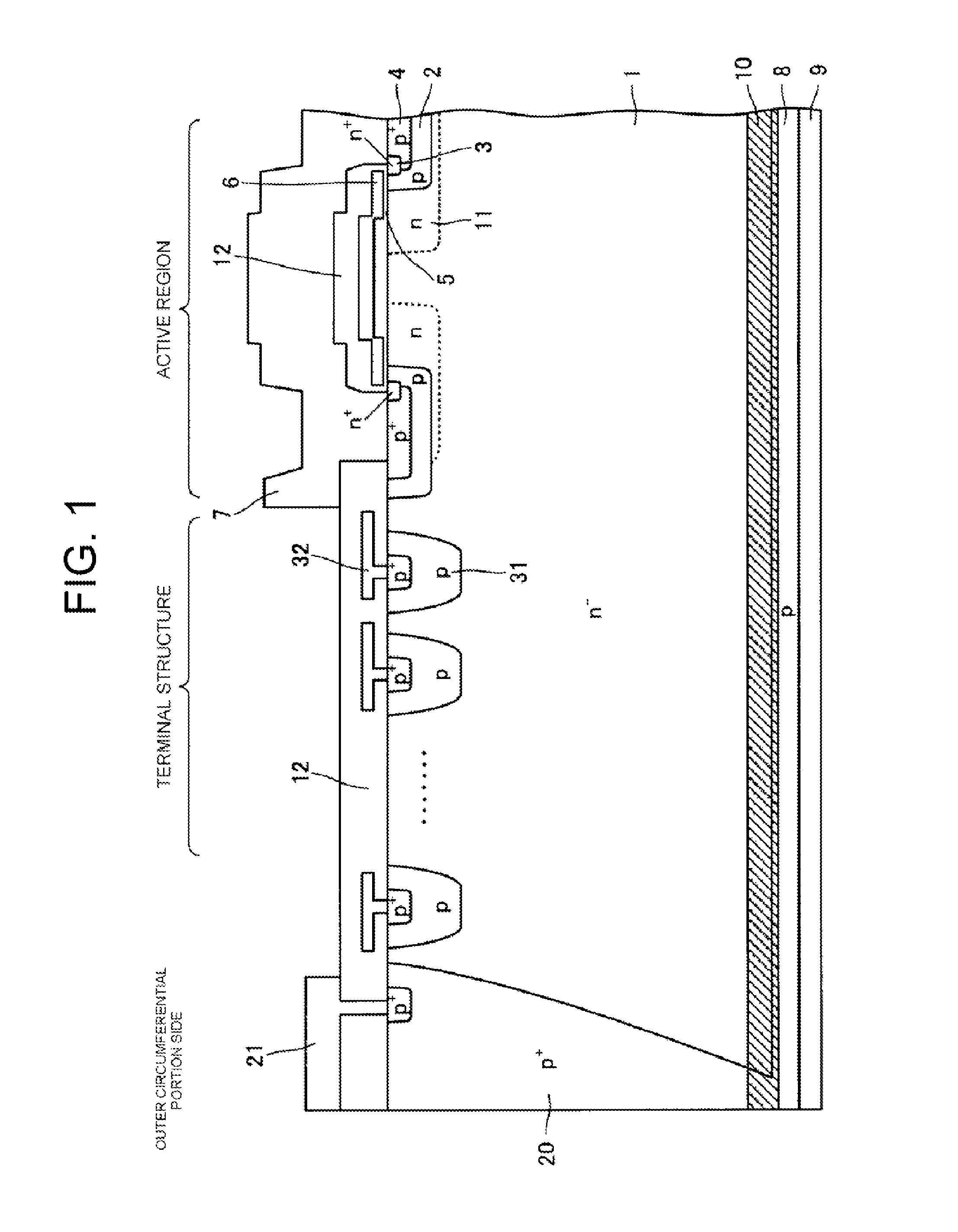
[0081]FIG. 1 is a sectional view showing the configuration of a semiconductor device according to Embodiment 1. The semiconductor device according to Embodiment 1 shown in FIG. 1 is an RB-IGBT which has a planar gate type MOS gate (insulated gate consisting of metal / oxide film / semiconductor) structure. As shown in FIG. 1, the semiconductor device according to Embodiment 1 has an active region and a terminal structure portion in an n− drift region (first semiconductor region) 1 consisting of an n− type semiconductor substrate (chip). A drift current flows into the active region which is surrounded by the terminal structure portion. The n− drift region 1 has a comparatively long carrier life time as compared with a typical device of an NPT structure. In the active region, a p base region (second semiconductor region) 2 is selectively provided in a surface layer of one side of the n− drift region 1.

[0082]An n region 11 is provided between the n− drift region 1 and the p base region 2. ...

embodiment 2

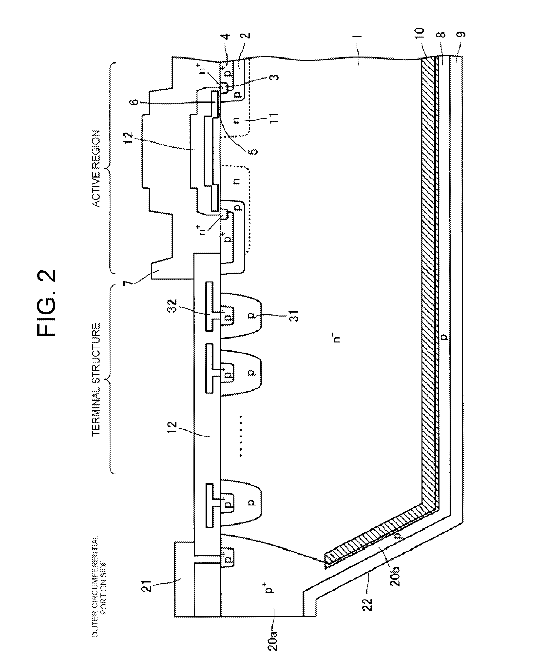
[0090]Next, the configuration of a semiconductor device according to Embodiment 2 will be described. FIG. 2 is a sectional view showing the configuration of a semiconductor device according to Embodiment 2. The semiconductor device according to Embodiment 2 is different from the semiconductor device according to Embodiment 1, in that grooves 22 are provided in the outer circumferential portion of the n− drift region 1, and the thickness of the n− drift region 1 is smaller on the outer circumferential portion side than on the active region side.

[0091]Specifically, as shown in FIG. 2, p+ isolation regions 20a are provided in the outer circumferential portion of the n− drift region 1 so as to extend from one side of the n− drift region 1 and at a smaller depth than the thickness of the n− drift region 1. In addition, grooves 22 are provided in the outer circumferential portion of the n− drift region 1 so as to extend from the other side of the n− drift region 1 and reach the p+ isolati...

embodiment 3

[0094]Next, a method for manufacturing a semiconductor device according to Embodiment 3 will be described in the case in which the semiconductor device according to Embodiment 2 is manufactured by way of example. FIGS. 3 to 5 are sectional views showing the state where the semiconductor device is being manufactured according to Embodiment 3. Here, a wafer is illustrated with the front surface up. However, the face of the wafer is reversed appropriately in each step (the same thing can be applied to FIGS. 6 to 19). First, as shown inFIG. 3, an n− type wafer serving as the n− drift region 1 (hereinafter referred to as “n− type wafer 1”) is prepared. Next, the p+ isolation regions 20a are selectively formed in the surface layer of the front surface of the n− type wafer 1 by ion injection of p type impurities and thermal diffusion treatment. The depth of each p+ isolation region 20a is set to be smaller than the final thickness of the n− type wafer 1.

[0095]Next, a front surface element ...


PUM


Abstract

An A-NPC circuit is configured so that the intermediate potential of two connected IGBTs is clamped by a bidirectional switch including two RB-IGBTs. Control is applied to the turn-on di / dt of the IGBTs during the reverse recovery of the RB-IGBTs. The carrier life time of an n− drift region in each RB-IGBT constituting the bidirectional switch is comparatively longer than that in a typical NPT structure device. A low life time region is also provided in the interface between the n− drift region and a p collector region, and extends between the n− drift region and the p collector region. Thus, it is possible to provide a low-loss semiconductor device, a method for manufacturing the semiconductor device and a method for controlling the semiconductor device, in which the reverse recovery loss is reduced while the reverse recovery current peak and the jump voltage peak during reverse recovery are suppressed.

Description

BACKGROUND OF THE INVENTION[0001]1. Field of the Invention[0002]The present invention relates to a semiconductor device, a method for manufacturing the semiconductor device, and a method for controlling the semiconductor device.[0003]2. Description of the Related Art[0004]High-voltage discrete semiconductors play a major role in power conversion equipment. For example, IGBTs (Insulated Gate Bipolar Transistors), MOSFETs (Metal Oxide Semiconductor Field Effect Transistors), FWDs (Free Wheeling Diodes), etc. are known as discrete semiconductors.[0005]IGBT on-state voltage drops due to conductivity modulation in a drift region. Due to this property, IGBTs are often used for applications to high-voltage equipment. RB-IGBTs (Reverse Blocking IGBTs) are also known. An RB-IGBT has a termination structure in which a pn junction between a collector region and a drift region of the IGBT is extended from the back surface of a semiconductor chip to the front surface thereof. In the RB-IGBT, a h...

Claims


Application Information

Patent Timeline
Patent Type & Authority Patents(United States)
IPC IPC(8): H01L29/739H01L21/8238H01L29/74H01L29/06H01L29/08H01L29/32H01L29/40H01L29/66H03K17/567H03K17/66
CPCH01L29/7395H03K17/66H01L29/66348H01L29/32H01L29/404H01L29/66333H01L29/0619H01L29/0661H01L29/0834H03K17/567H01L29/0657H01L29/0847H01L29/42368H02M7/487
Inventor LU, HONG-FEI
Owner FUJI ELECTRIC CO LTD
Why Eureka
Try Eureka