

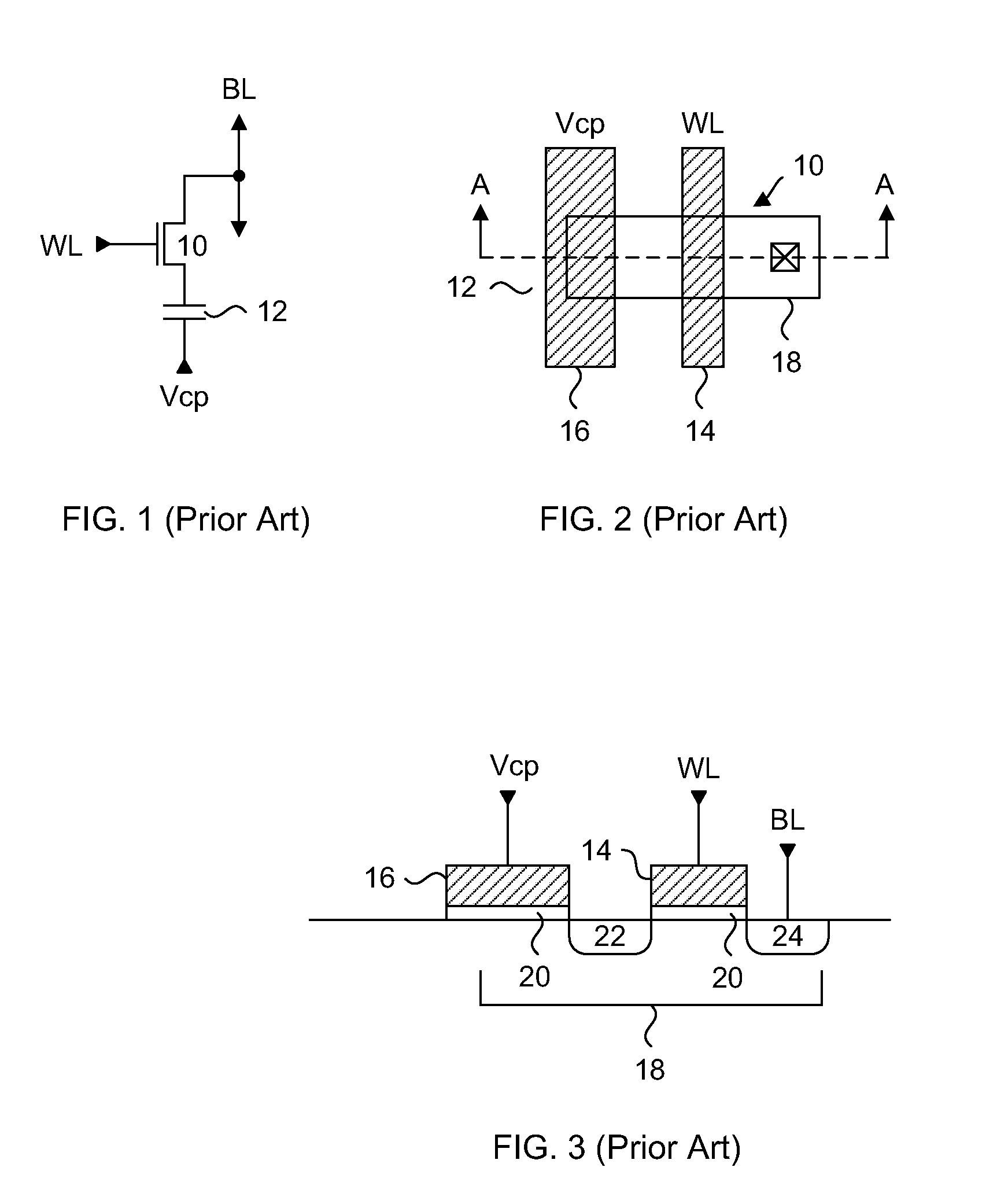
Low VT antifuse device
a low-voltage, anti-fuse technology, applied in semiconductor devices, semiconductor/solid-state device details, electrical apparatus, etc., can solve the problems of affecting the proper operation of the single-transistor anti-fuse memory cell, the redesign incurs significant cost overhead, and the leakage of salicided transistors, so as to reduce and achieve the effect of reducing the risk of forming defects
- Summary
- Abstract
- Description
- Claims
- Application Information
AI Technical Summary
Benefits of technology
Problems solved by technology
Method used
Image

Examples
Embodiment Construction
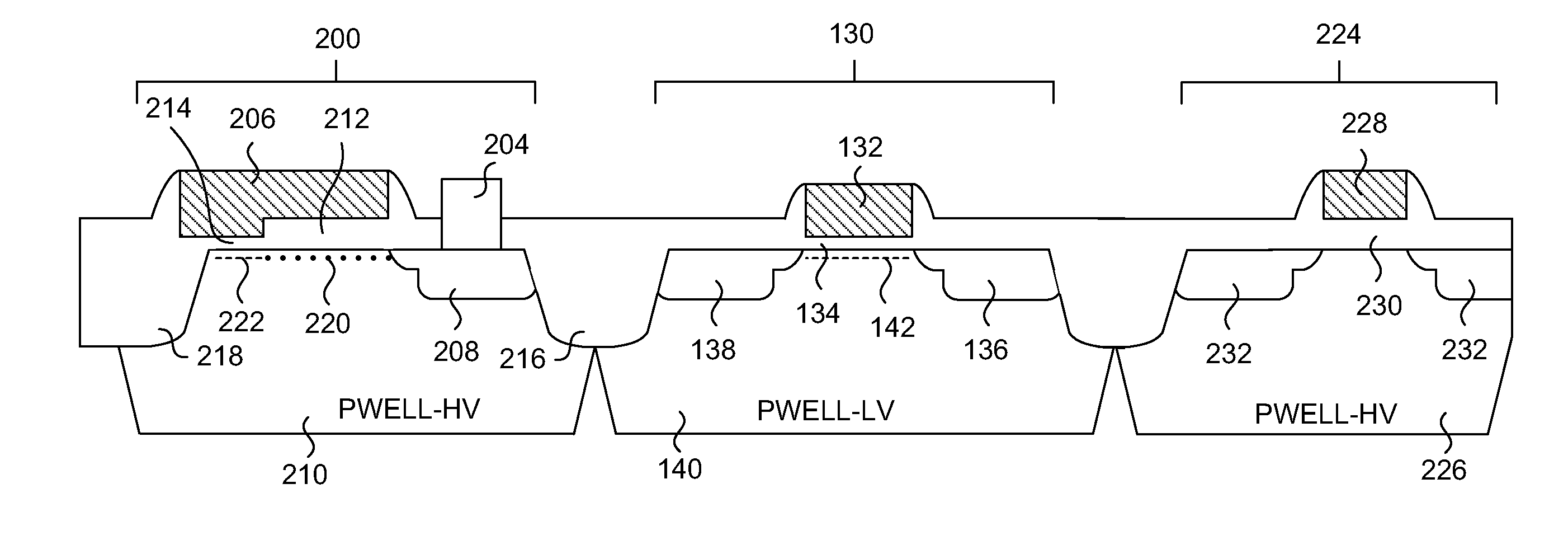
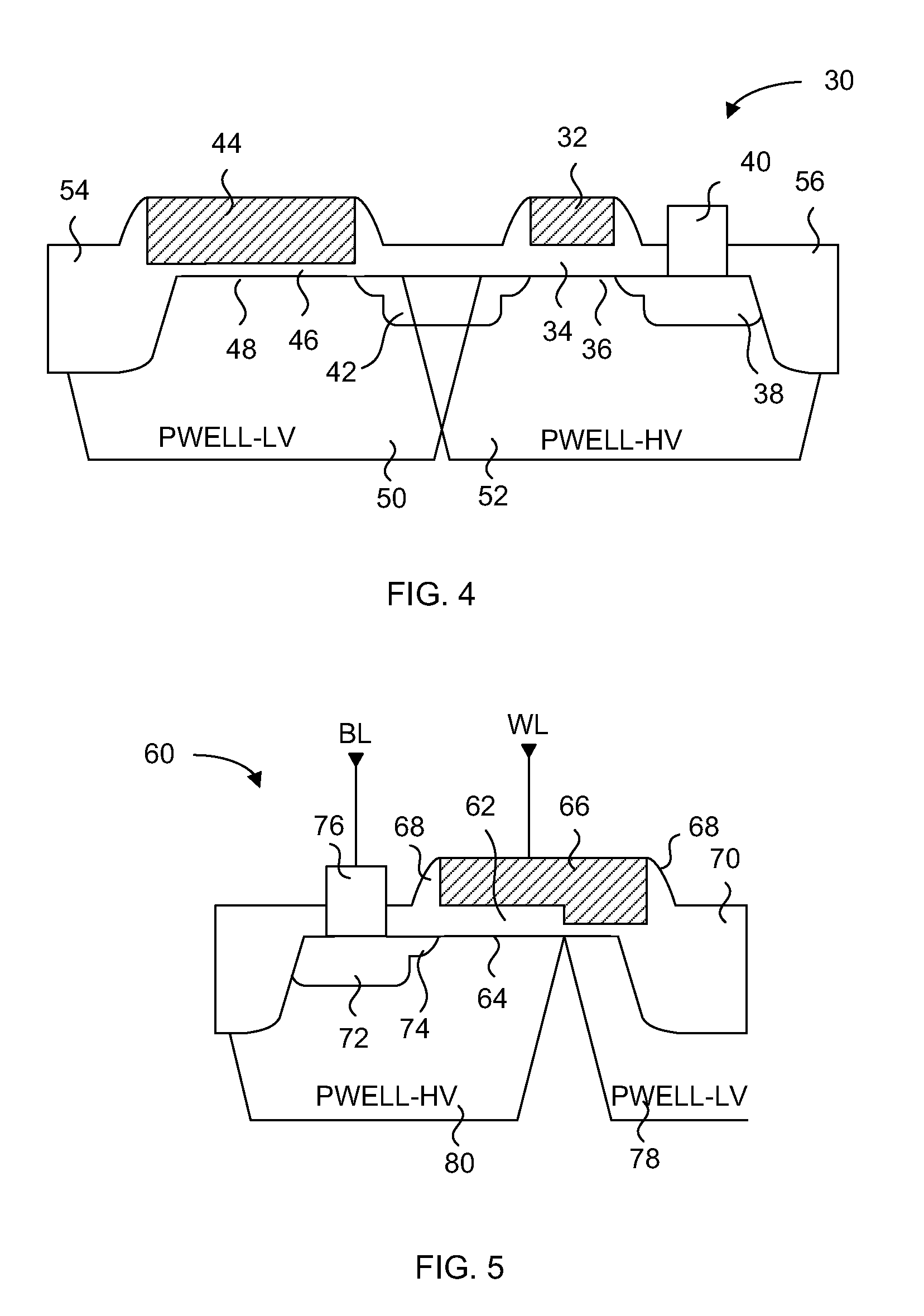
[0046]The embodiments of the present invention describe a one time programmable memory cell having an anti-fuse device with a low threshold voltage independent of core circuit process manufacturing technology. A two transistor memory cell having a pass transistor and an anti-fuse device, or a single transistor split channel memory cell having a dual thickness gate oxide, are formed in a high voltage well that is used for forming high voltage transistors. The threshold voltage of the anti-fuse device differs from the threshold voltages of any transistor in the core circuits of the memory device, but has a gate oxide thickness that is the same as a transistor in the core circuits. The pass transistor has a threshold voltage that differs from the threshold voltages of any core circuit transistor, and has a gate oxide thickness that differs from any transistor in the core circuits.
[0047]In particular, the embodiments of the present invention achieve a low programmed anti-fuse device thr...
PUM
 Abstract
Description
Claims
Application Information