Semiconductor device

a technology of semiconductor devices and shielding circuits, applied in emergency protective circuit arrangements, emergency protection circuit arrangements, etc., can solve the problems of unstable operation of semiconductor devices, low surge immunity, and the protection circuit itself may break, so as to stabilize the power supply potential or the potential of a signal , the area of the protection circuit can be small

Inactive Publication Date: 2015-01-27
SEMICON ENERGY LAB CO LTD
View PDF128 Cites 17 Cited by
  • Summary
  • Abstract
  • Description
  • Claims
  • Application Information

AI Technical Summary

Benefits of technology

[0010]With the progress of miniaturization and integration of a semiconductor device, it is desired to reduce the area of a protection circuit. However, miniaturization of an element used in the protection circuit may lower the surge immunity and thereby the protection circuit itself may break in some cases.
[0012]An object of an embodiment of the present invention is to provide a protection circuit having a small area and redundancy. Further, another object is to provide a protection circuit with small leak current.
[0017]Transistors including silicon in their respective channel formation regions can be used as the first nonlinear element and the second nonlinear element. Transistors including a compound semiconductor in their respective channel formation regions can be used as the third nonlinear element and the fourth nonlinear element. In particular, when an oxide semiconductor is used as the compound semiconductor, the off-state current of the transistors can be extremely small. Accordingly, when the transistors are used in the protection circuit connected between the wirings, the leak current between the wirings can be reduced.
[0020]A protection circuit which is an embodiment of the present invention has a structure in which a plurality of nonlinear elements is stacked, whereby the area of the protection circuit can be small. Further, since the plurality of nonlinear elements is electrically connected in series, the protection circuit has redundancy for short-circuit defects. By using a transistor including an oxide semiconductor as at least one of the nonlinear elements in the protection circuit, leak current between wirings, between which the protection circuit is connected, can be reduced; as a result, the power supply potential or the potential of a signal can be stabilized.

Problems solved by technology

However, miniaturization of an element used in the protection circuit may lower the surge immunity and thereby the protection circuit itself may break in some cases.
Therefore, in the case where a protection circuit including such an element is connected between a wiring (e.g., a signal line) connected to a semiconductor circuit and a power supply line, a leak current may flow between the wirings to change the potentials of the wirings or the power supply potential, causing unstable operation of the semiconductor device.

Method used


Image

  • Semiconductor device
  • Semiconductor device
  • Semiconductor device

Examples


embodiment 1

(Embodiment 1)

[0052]In this embodiment, a configuration of protection circuits used in a semiconductor device according to an embodiment of the present invention and an operation method of the protection circuits will be described.

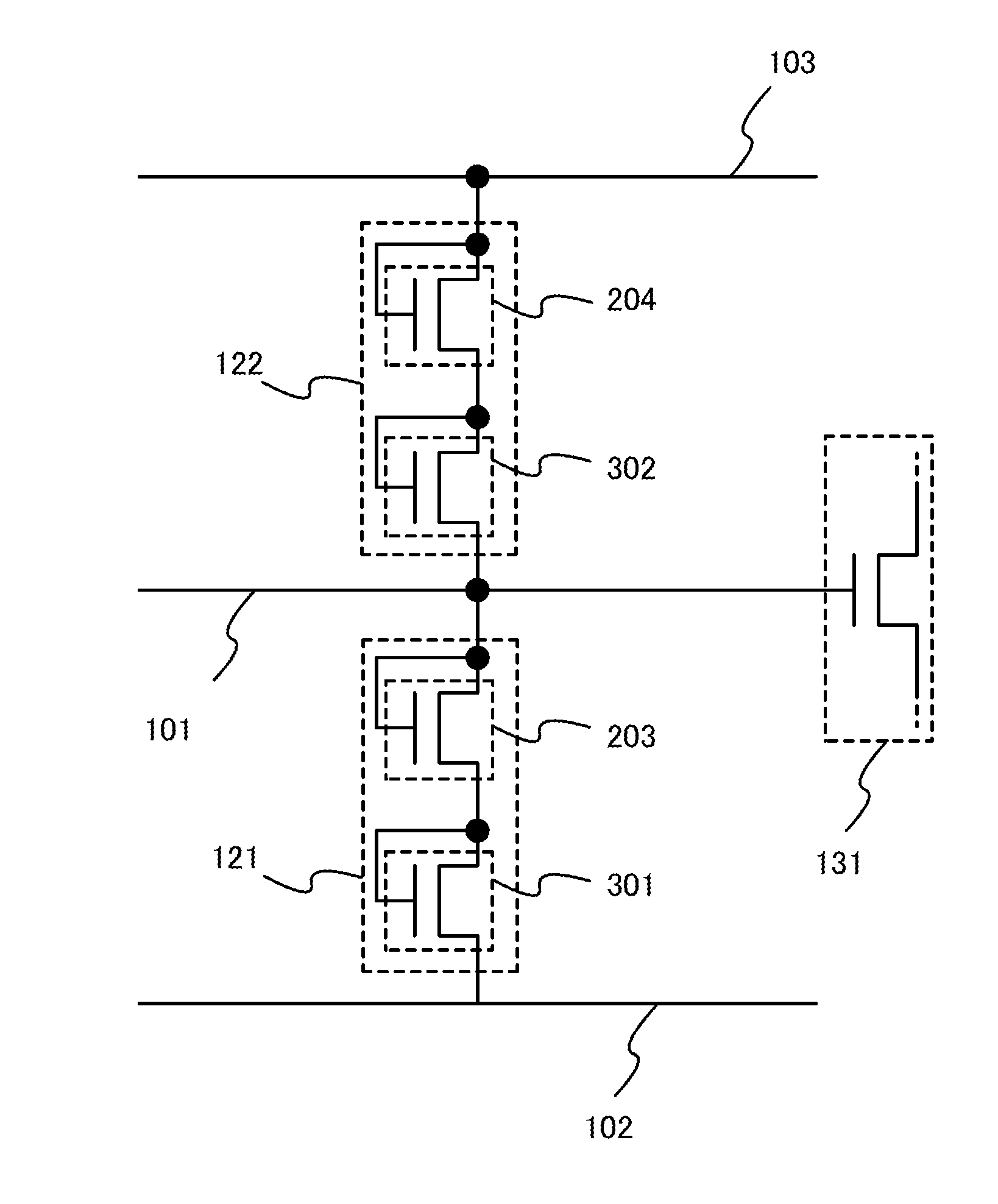
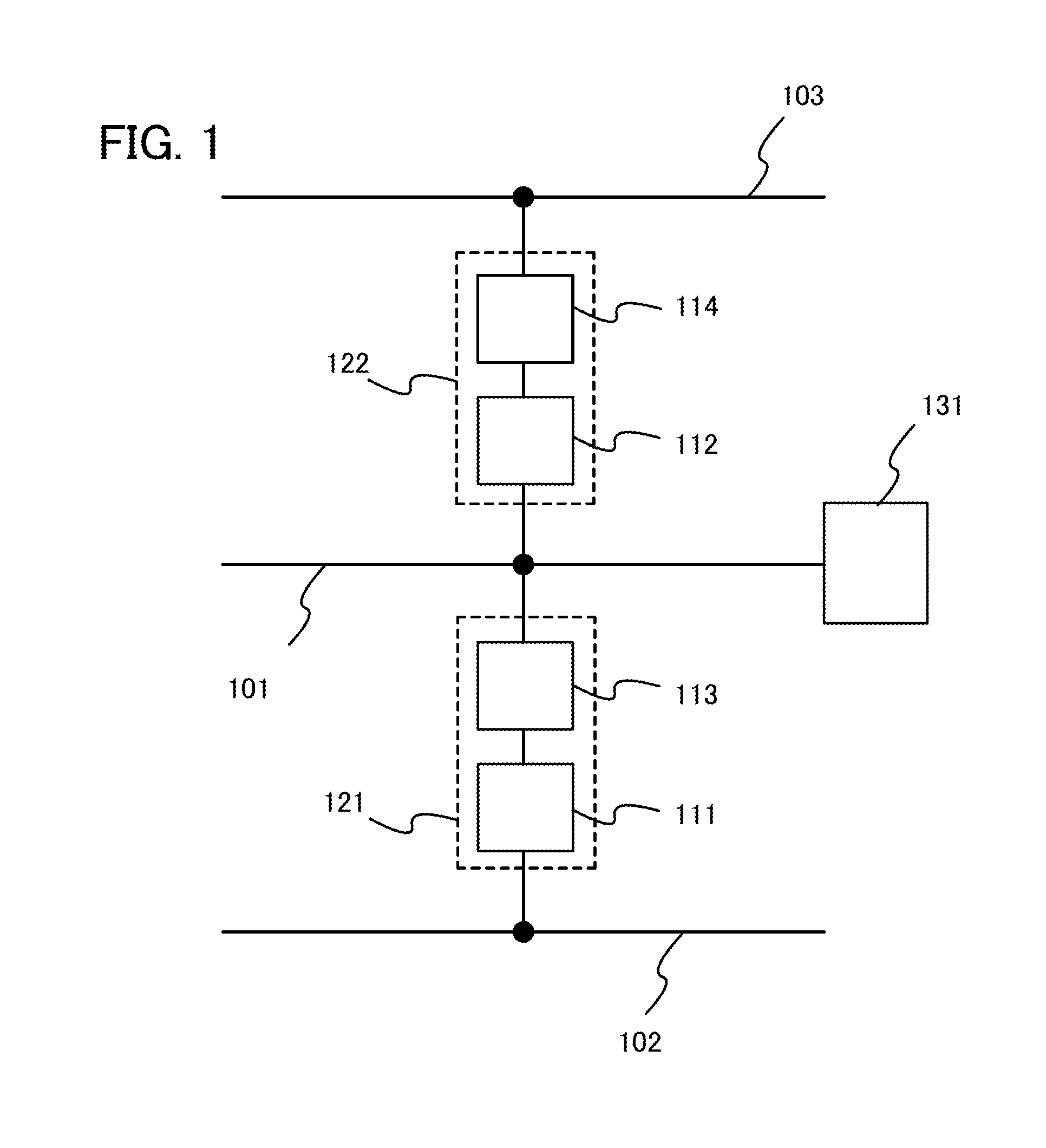
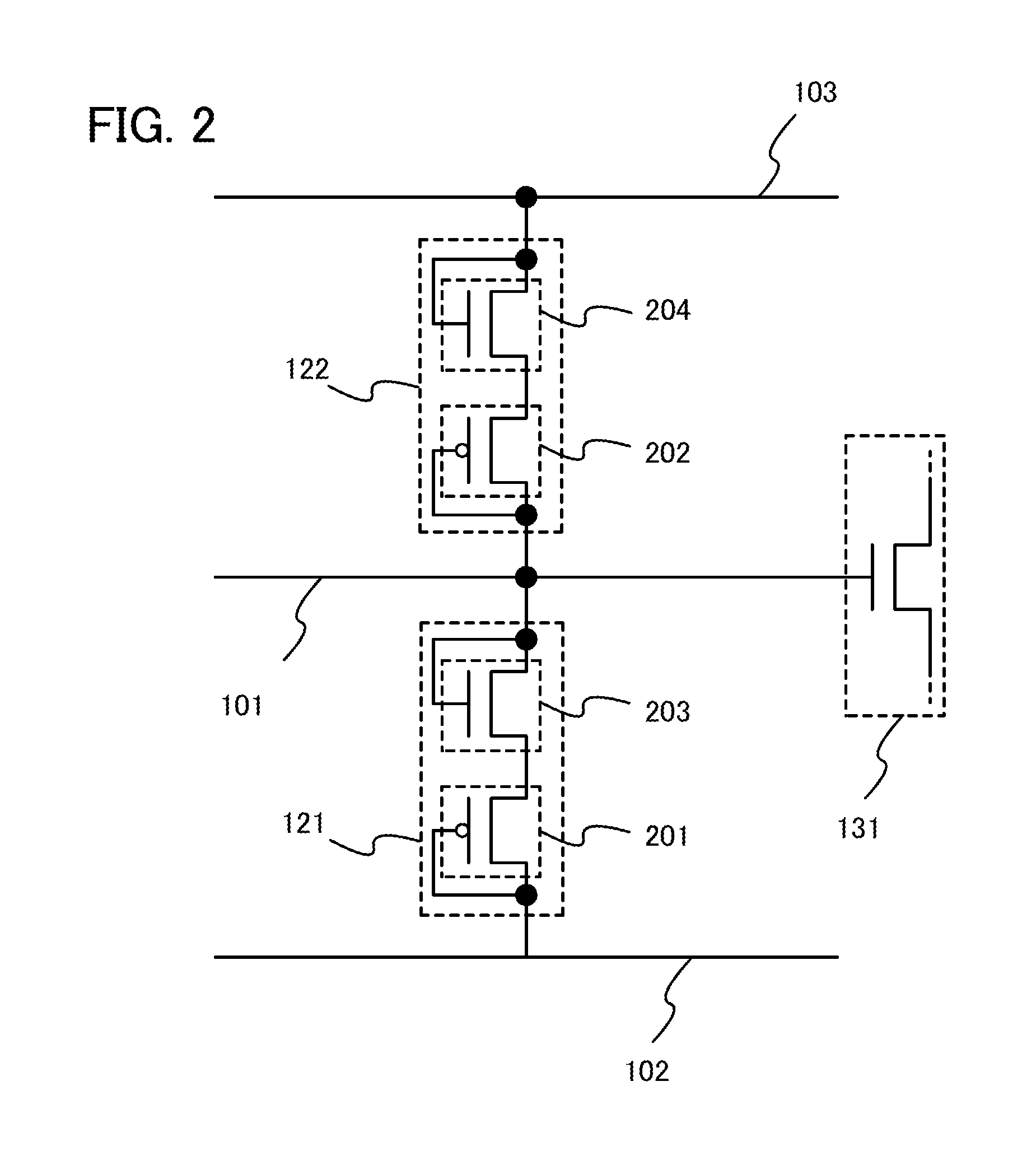
[0053]FIG. 1 illustrates protection circuits used in a semiconductor device according to an embodiment of the present invention and a mode of connection between the protection circuits and wirings. A first protection circuit 121 includes a first nonlinear element 111 and a third nonlinear element 113. A second protection circuit 122 includes a second nonlinear element 112 and a fourth nonlinear element 114. The semiconductor device according to an embodiment of the present invention includes a first wiring 101 connected to a semiconductor circuit 131, a second wiring 102, and a third wiring 103. The first protection circuit 121 is electrically connected between the first wiring 101 and the second wiring 102, and the second protection circuit 122 is electri...

embodiment 2

(Embodiment 2)

[0074]In this embodiment, an example of a method for manufacturing the protection circuits described in Embodiment 1 will be described. Note that in this embodiment, a method for manufacturing top-gate transistors including an oxide semiconductor in a non-self-aligned manner will be described as an example. However, the structure of the transistor is not limited thereto, and top-gate transistors may be manufactured in a self-aligned manner or bottom-gate transistors may be manufactured.

[0075]First, an element formation region isolated with an insulating layer 540 (also referred to as a field oxide film) is formed in a single crystal silicon substrate 500. An element isolation region can be formed by local oxidation of silicon (LOCOS), shallow trench isolation (STI), or the like.

[0076]Here, the substrate is not limited to the single crystal silicon substrate. A silicon on insulator (SOI) substrate or the like can be used as well.

[0077]Next, a first insulating layer 536 ...

embodiment 3

(Embodiment 3)

[0163]In this embodiment, a structure of a transistor, which is different from the structure described in the method for manufacturing a transistor including an oxide semiconductor in Embodiment 2 and which can be applied to the third nonlinear element 203 and the fourth nonlinear element 204 in Embodiments 1 and 2, will be described.

[0164]A transistor 901 illustrated in FIG. 8A includes, over an insulating layer 902, an oxide semiconductor layer 903 which functions as an active layer; a source electrode 904 and a drain electrode 905 which are formed over the oxide semiconductor layer 903; a gate insulating layer 906 over the oxide semiconductor layer 903, the source electrode 904, and the drain electrode 905; and a gate electrode 907 which is provided over the gate insulating layer 906 so as to overlap with the oxide semiconductor layer 903.

[0165]The transistor 901 illustrated in FIG. 8A is a top-gate transistor in which the gate electrode 907 is formed over the oxide...


PUM


Abstract

To provide a protection circuit having a small area, redundancy, and small leak current. In the protection circuit, a plurality of nonlinear elements is provided so as to overlap with each other and so as to be electrically connected in series. At least one nonlinear element in the protection circuit is a diode-connected transistor including an oxide semiconductor in its channel formation region. The other nonlinear element is a diode-connected transistor including silicon in its channel formation region or a diode including silicon in its junction region.

Description

BACKGROUND OF THE INVENTION[0001]1. Field of the Invention[0002]The present invention relates to a semiconductor device including a means for preventing a circuit from being damaged by application of unexpected high voltage due to electrostatic discharge or the like. Note that “semiconductor device” in this specification indicates all devices that can operate by utilizing semiconductor characteristics. For example, a display device, an imaging device, a memory device, an arithmetic device, and electronic devices using such devices are all semiconductor devices.[0003]2. Description of the Related Art[0004]In a semiconductor circuit used in a semiconductor device, a semiconductor element, an electrode, or the like could be damaged by electrostatic discharge (hereinafter referred to as “ESD”). As a measure to prevent damage of a semiconductor circuit due to ESD, a protection circuit is connected to a semiconductor circuit in many cases. A protection circuit refers to a circuit for prev...

Claims


Application Information

Patent Timeline
Patent Type & Authority Patents(United States)
IPC IPC(8): H02H3/22H01L27/02H01L27/06
CPCH01L27/0266H01L27/0688
Inventor TOMATSU, HIROYUKI
Owner SEMICON ENERGY LAB CO LTD
Why Eureka
Try Eureka