Semiconductor device and operation method for same

a technology of semiconductor devices and mask sets, which is applied in semiconductor devices, digital storage, instruments, etc., can solve the problems of physical limit of devices, steep rise in the price of mask sets, and steep rise in the cost of lithography processes, and achieve low-voltage operation and high reliability.

Active Publication Date: 2015-06-16
NANOBRIDGE SEMICON INC
View PDF24 Cites 1 Cited by
  • Summary
  • Abstract
  • Description
  • Claims
  • Application Information

AI Technical Summary

Benefits of technology

[0021]According to the present invention, it is possible to realize the semiconductor device which can achieve the high reliability and perform low-voltage operation.

Problems solved by technology

The steep rise in the cost of the lithography process is, for example, a steep rise in the prices of an apparatus and a mask set.
The physical limit to the device size is, for example, a limit to the operation and a limit due to the manufacturing deviation.

Method used


Image

  • Semiconductor device and operation method for same
  • Semiconductor device and operation method for same
  • Semiconductor device and operation method for same

Examples


first exemplary embodiment

(Modified Example )

[0064]FIG. 4(A) is a modified example of the semiconductor device shown in FIG. 3(A). FIG. 4(B) shows the structure of the semiconductor device, while FIG. 4(A) shows a circuit diagram of the semiconductor device. As shown in FIG. 4(A), it is possible to unify the first electrode 11 of the first switching element 1 with the first electrode 21 of the second switching element 2. Because of the constitution, it becomes possible to miniaturize the semiconductor device, and to reduce transmission loss of a control signal. Moreover, it is also possible to unify the ion conductor 13 of the first switching element 1 with the ion conductor 23 of the second switching element 2 as shown in FIG. 5 as long as the first electrodes of the first switching element and the second switching element are electrically connected each other.

(Programming Method of Switching Element)

[0065]The method for programming the switching element according to the first exemplary embodiment will be d...

fourth exemplary embodiment

(Modified Example of Fourth Exemplary Embodiment)

[0078]FIG. 10(A) is a modified example of the semiconductor device shown in FIG. 9(A). FIG. 10(B) shows a structure of the semiconductor device, while FIG. 10(A) shows a circuit diagram of the semiconductor device. As shown in FIG. 10(A), it is possible to unify the second electrode 12 of the first switching element 1 and the second electrode 22 of the second switching element 2. By the constitution, it is possible to miniaturize the semiconductor device, and to reduce transmission loss of a control signal. As long as the second electrodes are electrically connected each other, it is also possible to unify the ion conductor 13 of the first switching element 1 and the ion conductor 23 of the second switching element 2 as shown in FIG. 11, for example.

(Programming Method of Switching Element)

[0079]The method for programming the switching element according to the fourth exemplary embodiment will be described below. FIG. 12 is a schematic...

example

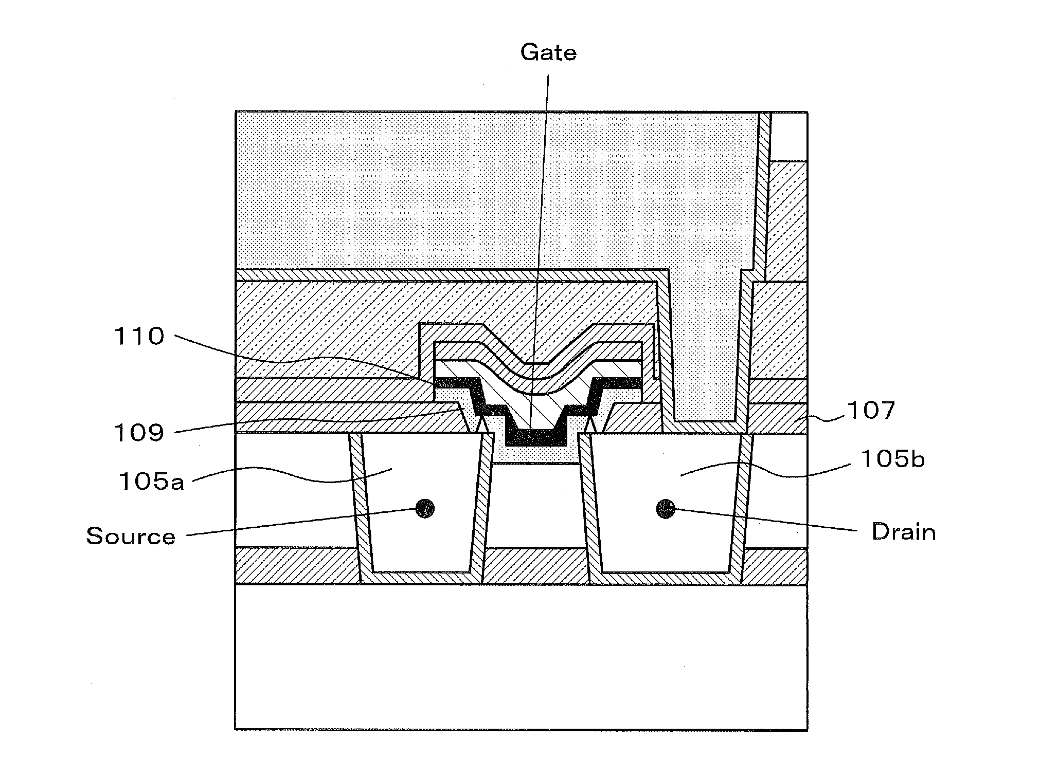
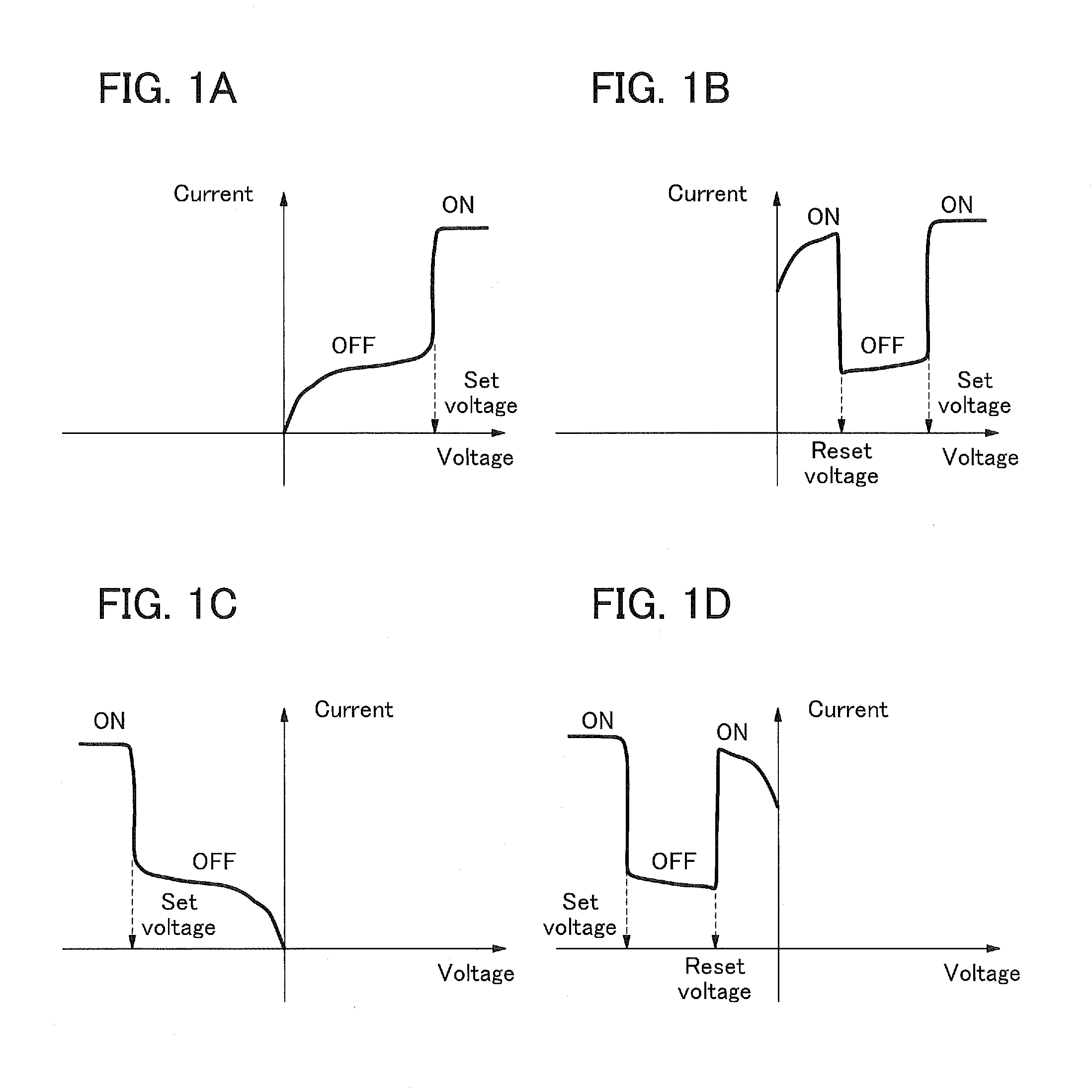
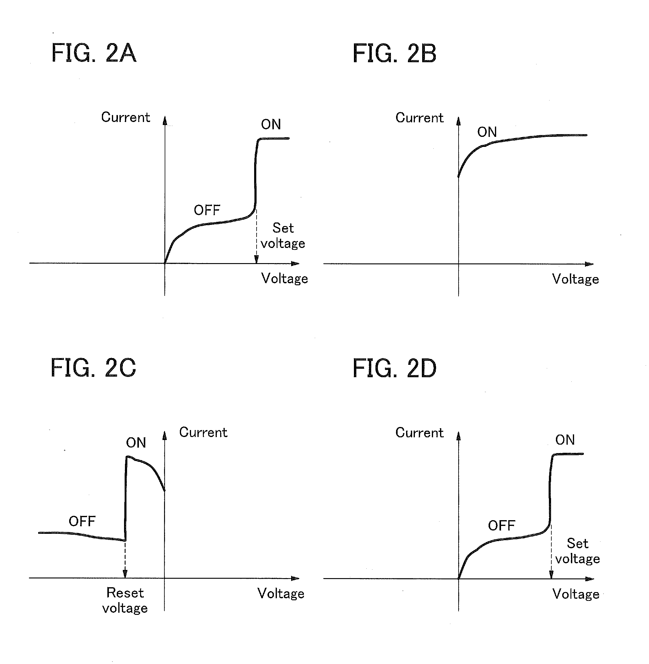
[0100]The semiconductor device according to the exemplary embodiment mentioned above has been implemented in the multi-layered wiring layer, and measure results on voltage versus current properties will be shown below.


PUM


Abstract

A semiconductor device includes a first switching element, a second switching element, and at least one third switching element; wherein the third switching element includes a first terminal and a second terminal, wherein each of the first switching element and the second switching element includes an ion conductor, a first electrode which is disposed so as to have contact with the ion conductor and supplies metal ions to the ion conductor, and a second electrode which is disposed so as to have contact with the ion conductor and is less susceptible to ionization than the first electrode; and wherein(a) the first electrode of the first switching element and the first electrode of the second switching element are electrically connected each other, and the first terminal of the third switching element is electrically connected to only the first electrodes which are electrically connected each other or(b) the second electrode of the first switching element and the second electrode of the second switching element are electrically connected each other, and the first terminal of the third switching element is electrically connected to only the second electrodes which are electrically connected each other.

Description

TECHNICAL FIELD[0001]The present invention relates to a semiconductor device and an operation method for the same, and particularly relates to a semiconductor device and an operation method for the same which use a variable resistance type nonvolatile element.BACKGROUND ART[0002]The semiconductor device, especially the silicon device has been progressed in the large scale integration and the low power consumption through applying the miniaturization (scaling rule: Moore's rule), and has been developed in a pace of four times progress every three years. It is required to improve device performance through applying an approach different from the conventional scaling rule, because the gate length of MOSFET (Metal Oxide Semiconductor Field Effect Transistor) nowadays has become shorter than 20 nm, a cost of the lithography process rises suddenly, and there exists physical limit to the device size. The steep rise in the cost of the lithography process is, for example, a steep rise in the...

Claims


Application Information

Patent Timeline
Patent Type & Authority Patents(United States)
IPC IPC(8): H01L29/06H01L27/24G11C13/00H01L27/10H01L45/00
CPCH01L27/2436G11C13/0007G11C13/0014G11C13/003G11C13/0069H01L27/101H01L27/2472G11C2013/0073H01L45/085H01L45/1233H01L45/1266H01L45/14H01L45/146H10B63/82H10B63/30H10N70/245H10N70/8416H10N70/881H10N70/826H10N70/8833H10B63/80
Inventor TADA, MUNEHIROMIYAMURA, MAKOTOHADA, HIROMITSU
Owner NANOBRIDGE SEMICON INC
Why Eureka
Try Eureka