
Manufacture method for a surface mounted power LED support and its product
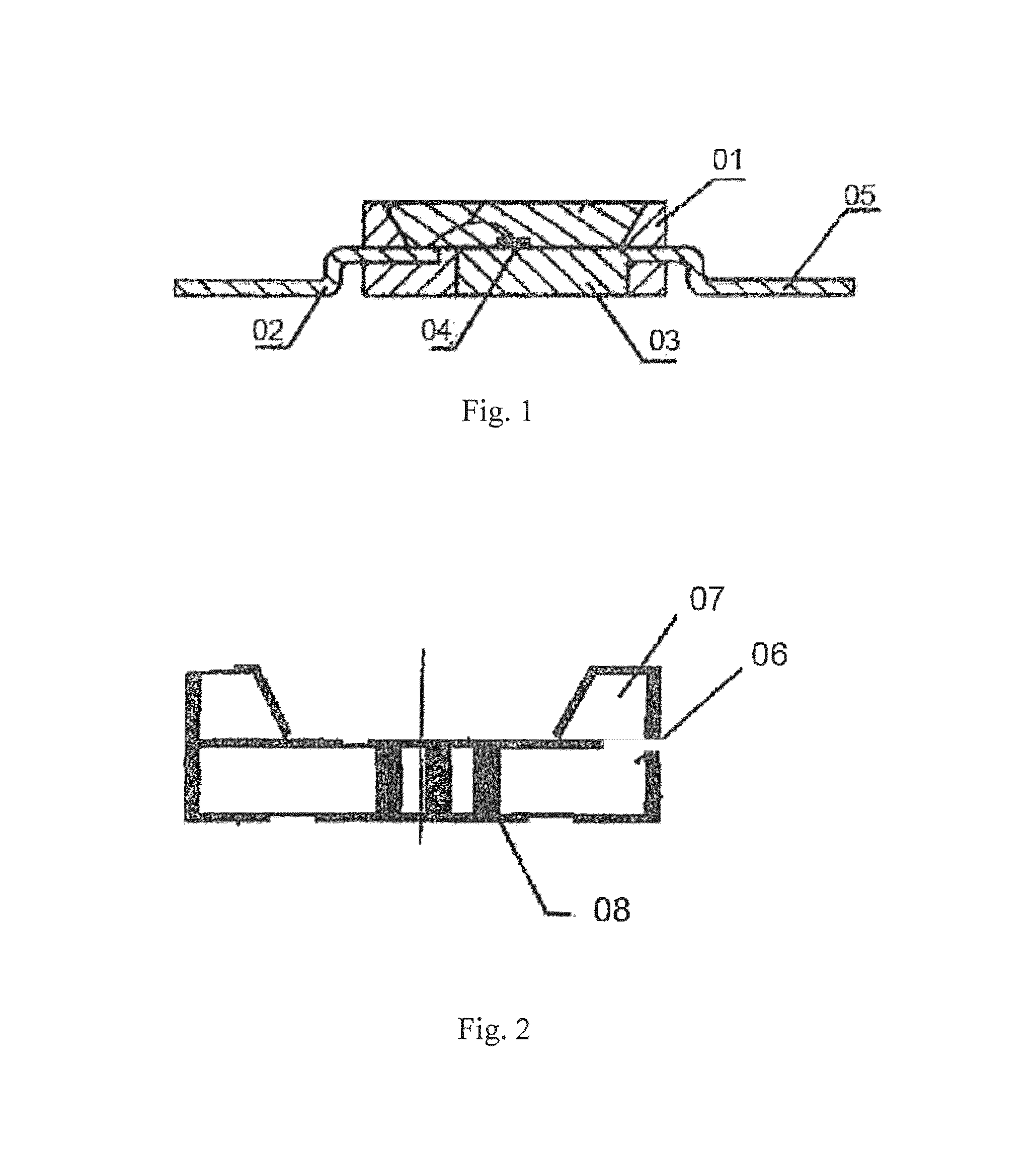
a manufacturing method and power led technology, applied in the direction of lighting and heating equipment, printed circuit non-printed electric components association, lighting support devices, etc., can solve the problems of poor universal applicability and low yield rate of ordinary insulating boards, and achieve high production efficiency, good product reliability, and simple processes
- Summary
- Abstract
- Description
- Claims
- Application Information
AI Technical Summary
Benefits of technology
Problems solved by technology
Method used
Image

Examples
first embodiment
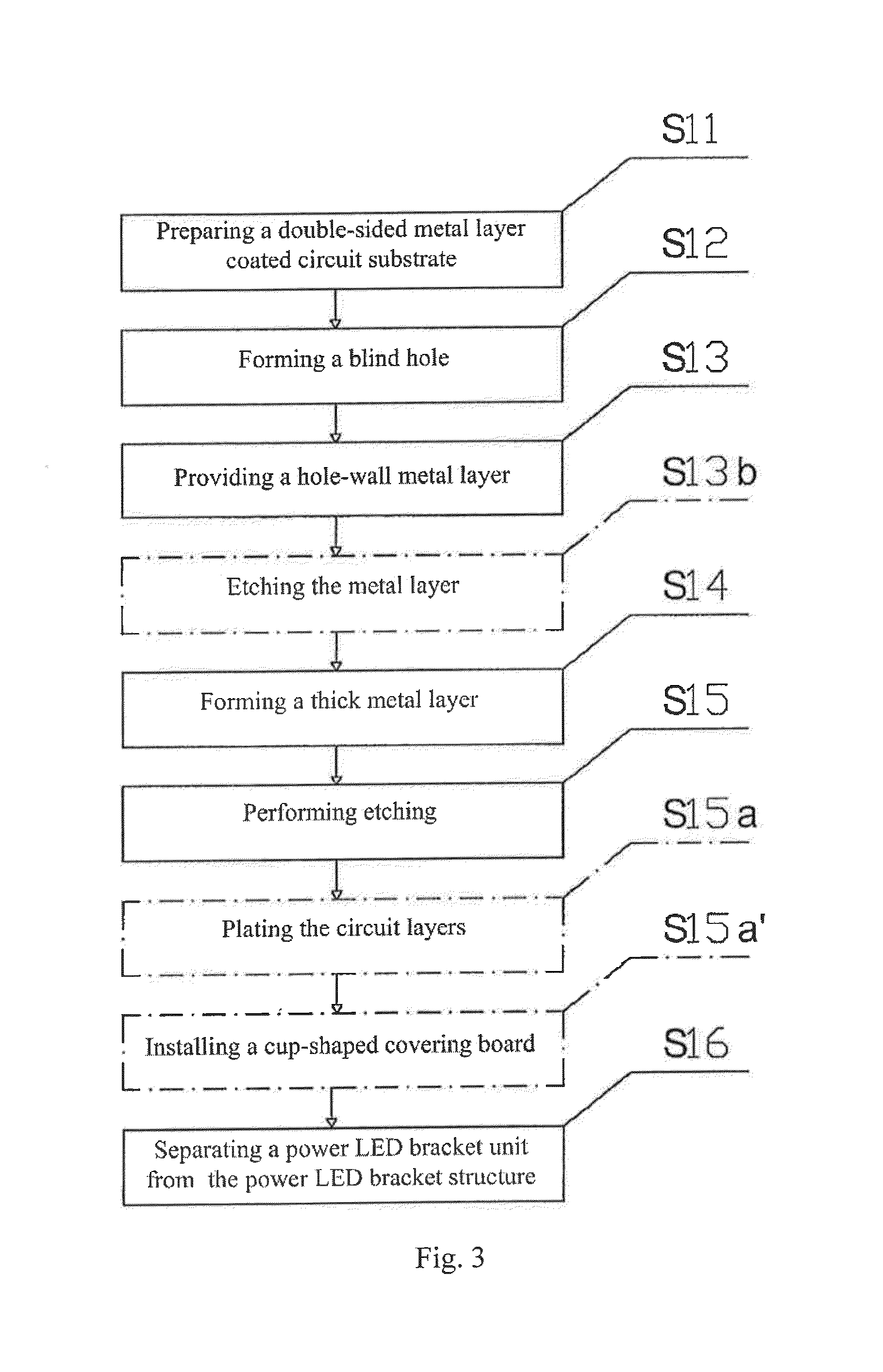
[0030]A method for manufacturing a power LED bracket according to the present application is shown in FIGS. 3 and 4. Manufacture steps of the embodiment are described in detail in conjunction with the process flow chart of the embodiment shown in FIG. 3 and the schematic view of the process steps shown in FIG. 4.
[0031]Step S11), preparing a double-sided metal layer coated circuit substrate: A double-sided metal layer coated circuit substrate 1 is prepared in advance. As shown in FIG. 4A, the circuit substrate 1 includes an ordinary insulating substrate 10, a first metal layer 11 coated on the upper surface of the substrate and a second metal layer 12 coated on the lower surface of the substrate 10. There is no special requirement on the material of the substrate 10. The substrate may be an ordinary insulating board such as a PCB board. Preferably, the substrate may be cheap materials, such as a fiber-glass cloth substrate, a CEM-3 (Composite Epoxy Material Grade-3) substrate, or a C...
second embodiment
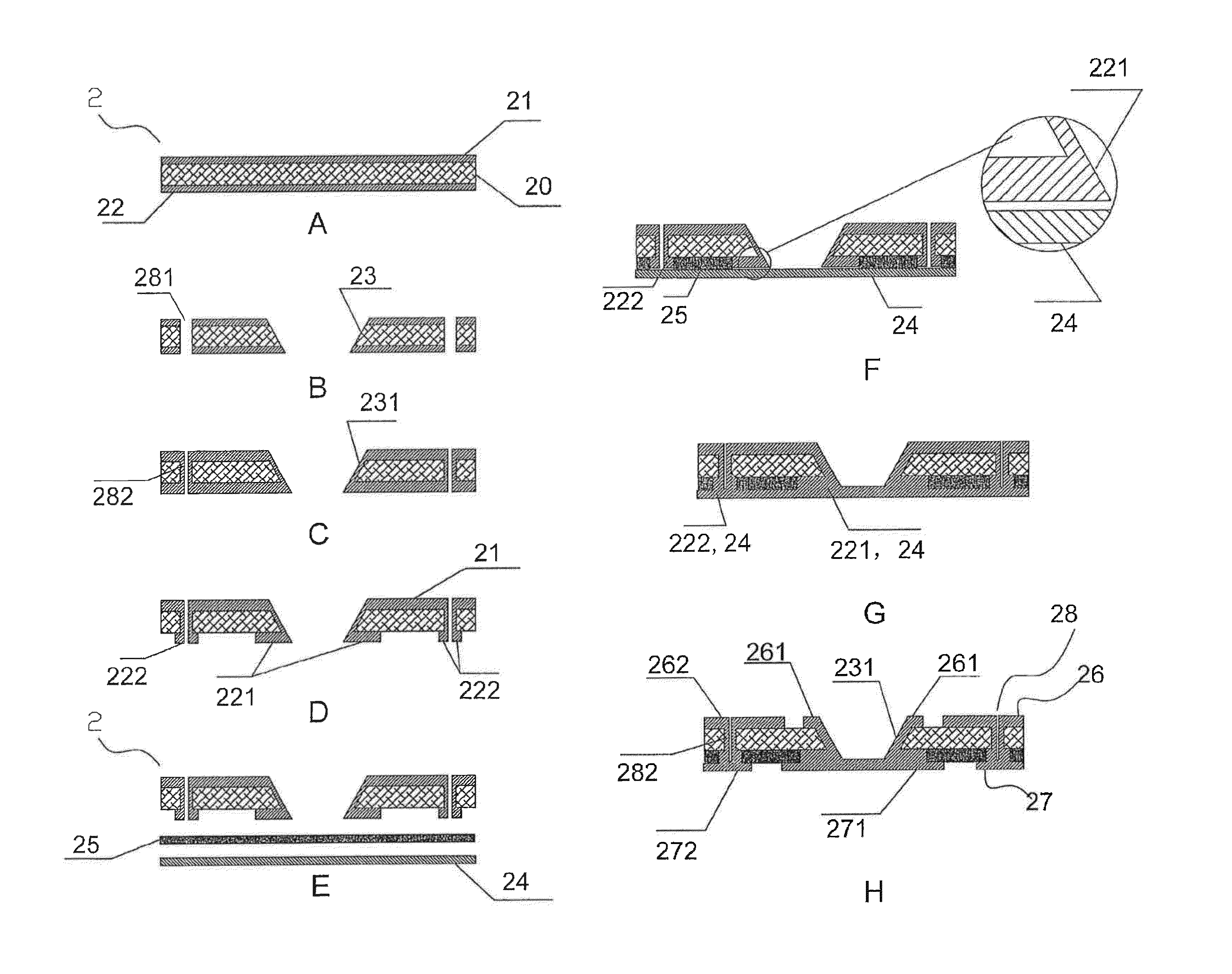
[0044]A method for manufacturing a power LED bracket according to the present application is shown in FIGS. 5 and 6. Manufacture steps of the embodiment are described in detail in conjunction with the process flow chart of the embodiment shown in FIG. 5 and the schematic view of process steps shown in FIG. 6.
[0045]Step S21), preparing a double-sided metal layer coated circuit substrate: A double-sided metal layer coated circuit substrate 2 is prepared in advance. The circuit substrate 2 includes an ordinary insulating substrate 20, a first metal layer 21 coated on the upper surface of the substrate and a second metal layer 22 coated on the lower surface of the substrate. There is no special requirement on the material of the substrate 20. The substrate may be an ordinary insulating board such as a PCB board. Preferably, the substrate may be cheap materials such as a fiber-glass cloth substrate (FR-4), a CEM-3 (Composite Epoxy Material Grade-3) substrate, or a CEM-1 (Composite Epoxy ...
third embodiment
[0060]A power LED bracket according to another of the present application is shown in FIG. 10. The power LED bracket of the present embodiment differs from the power LED bracket by further including a cup-shaped covering board 45 provided on the upper surface of the bracket substrate 4. The cup-shaped covering board 45 is connected to the upper surface of the bracket substrate 4 via an adhesive film 46, and further includes a cup hole 451 corresponding to the position of the blind hole 41. A diameter of the cup hole 451 is larger than a diameter of the blind hole 41, with the lead connecting portion 431 being exposed in the cup hole 451 and the positive and negative electrode 42 being covered by the cup-shaped covering board 45. The cup-shaped covering board 45 may be of a reflection cup shape or a cylindrical shape, and is not limited to the present embodiment. In other embodiments, the upper surface of the cup-shaped covering board 45 may be coated with a black material to increa...
PUM
| Property | Measurement | Unit |
|---|---|---|
| thickness | aaaaa | aaaaa |
| thick | aaaaa | aaaaa |
| conductive | aaaaa | aaaaa |
Abstract
Description
Claims
Application Information