Supercharge Your Innovation With Domain-Expert AI Agents!

Photoelectric conversion device

a conversion device and photoelectric technology, applied in the field of photoelectric conversion devices, can solve the problems of light loss caused by and achieve the effect of small light loss due to light absorption in the window layer and high conversion efficiency

Inactive Publication Date: 2015-10-13
SEMICON ENERGY LAB CO LTD
View PDF39 Cites 0 Cited by
  • Summary
  • Abstract
  • Description
  • Claims
  • Application Information

AI Technical Summary

Benefits of technology

This configuration significantly reduces light loss in the window layer, improves photoelectric conversion efficiency, and extends the optical path length, leading to enhanced electric characteristics and increased short-circuit current.

Problems solved by technology

In the above photoelectric conversion device, since crystalline silicon or amorphous silicon is used for a window layer, the light loss due to light absorption in the window layer is caused.

Method used


Image

  • Photoelectric conversion device
  • Photoelectric conversion device
  • Photoelectric conversion device

Examples


embodiment 1

[0037]In this embodiment, a photoelectric conversion device according to one embodiment of the present invention and a method for manufacturing the photoelectric conversion device will be described.

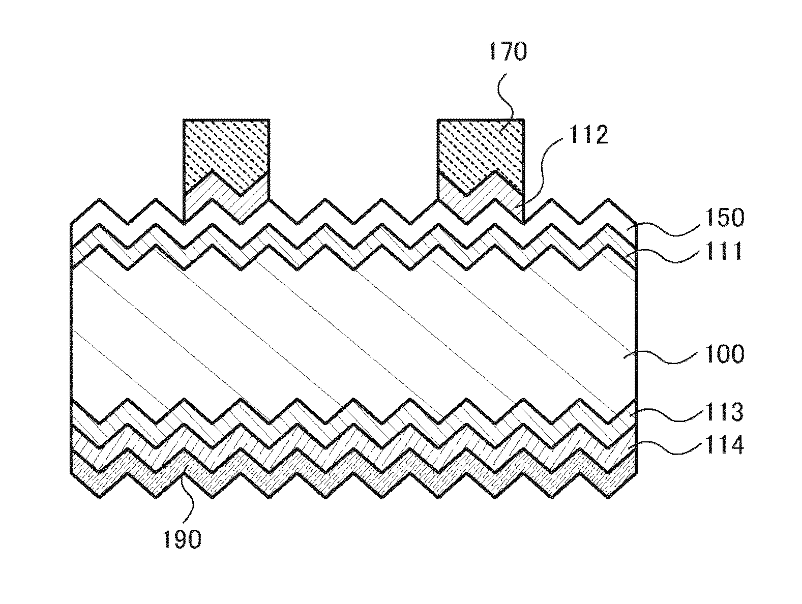
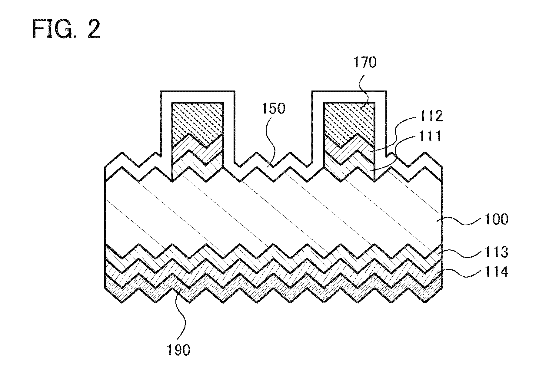
[0038]FIG. 1A is a cross-sectional view of a photoelectric conversion device according to one embodiment of the present invention. The photoelectric conversion device includes a crystalline silicon substrate 100 and further includes, over one surface of the crystalline silicon substrate, a first silicon semiconductor layer 111, a light-transmitting semiconductor layer 150, a second silicon semiconductor layer 112, and a first electrode 170. Furthermore, the photoelectric conversion device includes a third silicon semiconductor layer 113 on the other surface of the crystalline silicon substrate, a fourth silicon semiconductor layer 114 formed on the third silicon semiconductor layer 113, and a second electrode 190 formed on the fourth silicon semiconductor layer 114. Note that the first el...

embodiment 2

[0090]In this embodiment, the light-transmitting semiconductor layer described in Embodiment 1 will be described.

[0091]For the light-transmitting semiconductor layer 150 in any of the photoelectric conversion devices described in Embodiment 1, a composite material of a transition metal oxide and an organic compound can be used. Note that, in this specification, the word “composite” means not only a state in which two materials are simply mixed but also a state in which a plurality of materials are mixed and charges are transferred between the materials.

[0092]As the transition metal oxide, a transition metal oxide having an electron-accepting property can be used. Specifically, among transition metal oxides, an oxide of a metal belonging to any of Groups 4 to 8 of the periodic table is preferable. In particular, it is preferable to use vanadium oxide, niobium oxide, tantalum oxide, chromium oxide, molybdenum oxide, tungsten oxide, manganese oxide, or rhenium oxide because of their hi...


PUM


Abstract

Provided is a photoelectric conversion device with high conversion efficiency in which the light loss due to light absorption in a window layer is significantly reduced by using a light-transmitting semiconductor layer comprising an organic compound and an inorganic compound. Specifically, the photoelectric conversion device includes: over one surface of a crystalline silicon substrate, a first silicon semiconductor layer; a light-transmitting semiconductor layer; a second silicon semiconductor layer which is partially formed on the light-transmitting semiconductor layer; and a first electrode. The photoelectric conversion device further includes: a third silicon semiconductor layer on the other surface of the crystalline silicon substrate; a fourth silicon semiconductor layer formed on the third silicon semiconductor layer; and a second electrode formed on the fourth silicon semiconductor layer. The light-transmitting semiconductor layer is formed using an organic compound and an inorganic compound, which contributes to the high light-transmitting property of the window layer.

Description

BACKGROUND OF THE INVENTION[0001]1. Field of the Invention[0002]The present invention relates to a photoelectric conversion device including a window layer formed using an organic compound and an inorganic compound.[0003]2. Description of the Related Art[0004]In recent years, photoelectric conversion devices that do not produce carbon dioxide during power generation have received attention as a measure against global warming. As typical examples thereof, solar cells have been known which use crystalline silicon substrates such as single crystalline and polycrystalline silicon substrates.[0005]In solar cells using a crystalline silicon substrate, a structure having so-called homo junction is widely used. In such a structure, a layer having the conductivity type opposite to that of the crystalline silicon substrate is formed on one surface side of the crystalline silicon substrate by diffusion of impurities.[0006]Alternatively, a structure with hetero junction in which amorphous silic...

Claims


Application Information

Patent Timeline
Patent Type & Authority Patents(United States)
IPC IPC(8): H01L31/0224H01L31/0747H01L31/20H01L51/42H01L51/00H10K99/00
CPCH01L51/4213H01L31/0747H01L31/202Y02E10/549H01L51/0053H01L51/0072Y02E10/547H01L51/006Y02P70/50H10K85/621H10K85/633H10K30/10H10K85/6572H10K30/50
Inventor YAMAZAKI, SHUNPEI
Owner SEMICON ENERGY LAB CO LTD
Features
  • R&D
  • Intellectual Property
  • Life Sciences
  • Materials
  • Tech Scout
  • Unparalleled Data Quality
  • Higher Quality Content
  • 60% Fewer Hallucinations
Learn More