Component and method for producing same

a technology of microelectromechanical system and components, applied in the direction of electromechanical transducers, instruments, transducer diaphragms, etc., can solve the problems of affecting the manufacturing method and manufacturing cost, the mounting surface of the package of this type is only very small, and the installation height is low, so as to achieve the effect of greatly simplifying the processing of the suppor

Active Publication Date: 2015-10-20
ROBERT BOSCH GMBH
View PDF5 Cites 0 Cited by
  • Summary
  • Abstract
  • Description
  • Claims
  • Application Information

AI Technical Summary

Benefits of technology

[0008]Based on the known wafer-based packaging concept, measures are proposed by the present invention via which, for a given chip surface area, the largest possible rear volume for the diaphragm structure of the MEMS component may be achieved. In addition, the processing of the support is greatly simplified by these measures.
[0010]Therefore, the chip or support surface area necessary for the feedthrough and the terminal pads for electrically contacting the MEMS component may be significantly reduced, in particular in favor of the cavity. For a component according to the present invention, the chip surface area necessary for electrically contacting the MEMS component is thus determined essentially only by the dimensions of the terminal pads.
[0014]The layout requirements as well as the sequence of the method steps in the processing of the plate-shaped support material according to the present invention allow the use of mechanical structuring processes such as drilling, milling, or lasering. Although these processes are associated with relatively large manufacturing tolerances, they are particularly cost-effective and may be easily adapted to the properties of various support materials. The large manufacturing tolerances of mechanical structuring processes do not have an adverse effect within the scope of the packaging concept according to the present invention, since in this case the size of the through openings for the via feedthroughs as well as the size of the cavity openings are noncritical. The absence of a dependency of the material on mechanical structuring processes during production of the cavity openings has proven to be particularly advantageous. Namely, in this structuring step, in addition to the support material the conductive material of the via feedthroughs must be removed when these via feedthroughs are cut.
[0017]In one specific embodiment of the packaging concept according to the present invention, the cavity adjoining the diaphragm structure of the MEMS component is implemented in the form of a through opening in the support. In applications which require a closed rear volume, such as microphone applications, the cavity may be easily closed with the aid of a base part which is either inserted into the through opening of the support or attached at the rear side of the support.
[0020]As previously described in conjunction with the related art, it has proven advantageous with respect to the miniaturization of the component as well as to cost-effective manufacture when the support is implemented in the form of an interposer system having essentially the same chip surface area as the MEMS component. The individual component elements, the MEMS component and the support, may then each be produced in the wafer composite, and optionally also mounted in the wafer composite. When the components are not separated until this point, the support and the MEMS element of a component automatically have essentially the same chip surface area.

Problems solved by technology

This extensive parallelization of chip manufacture and packaging is extremely efficient, which affects the manufacturing method and the manufacturing costs.
Packages of this type require only a very small mounting surface, i.e., printed circuit board space, and have a very low installation height.
This configuration of the feedthroughs is at the expense of the lateral cavern extension for a given chip size.
In addition, the processing of a cap wafer including a cavern which is closed on the rear side and completely or partially filled feedthroughs is relatively complicated.

Method used


Image

  • Component and method for producing same
  • Component and method for producing same
  • Component and method for producing same

Examples


Embodiment Construction

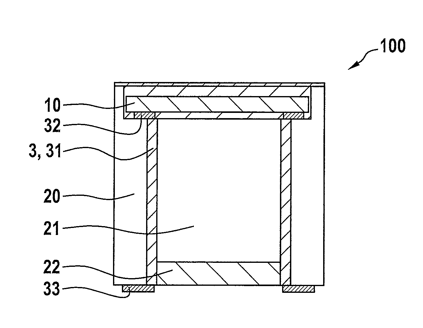
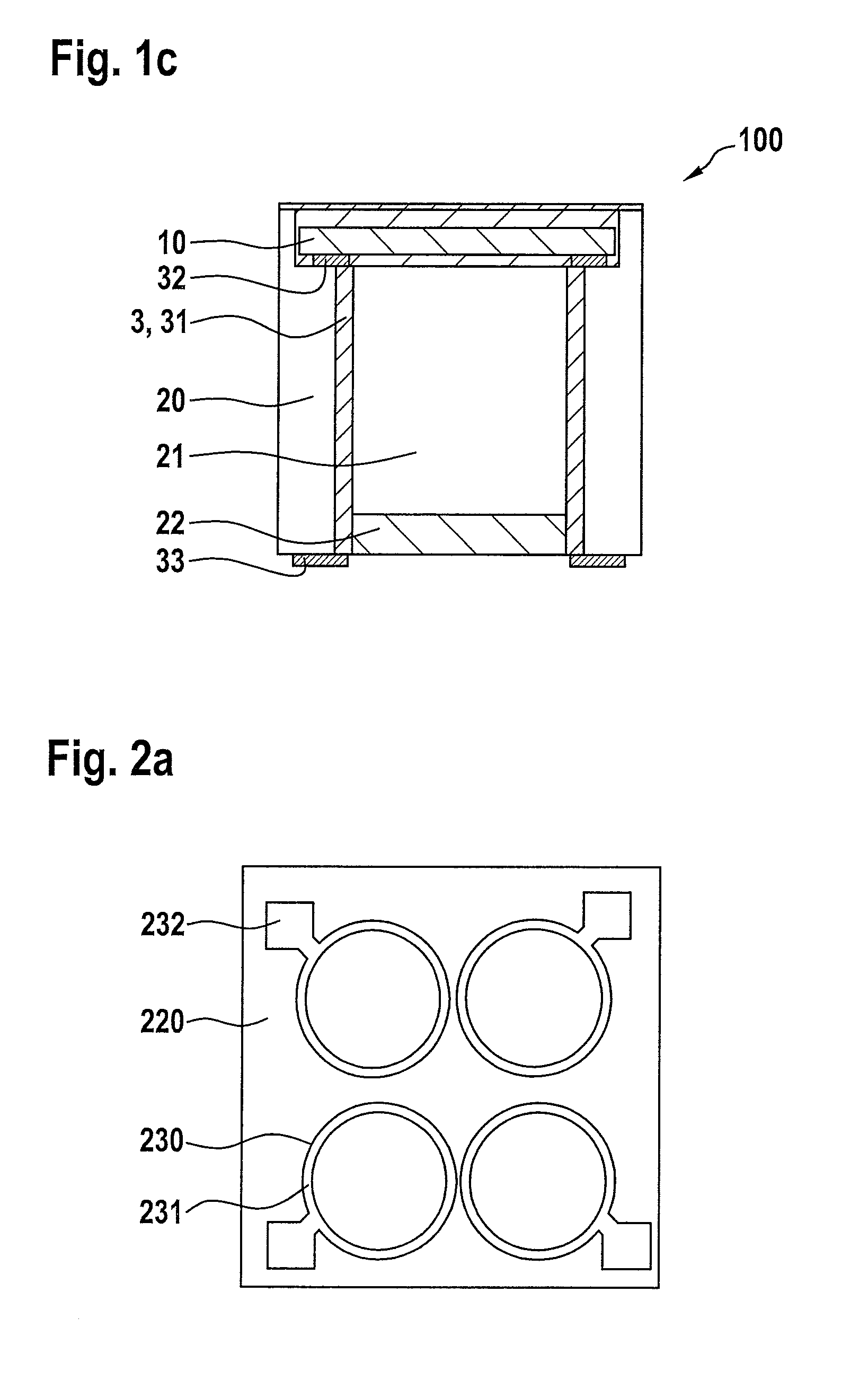
[0028]As described above, the packaging concept according to the present invention for MEMS components, having a diaphragm structure formed in the front side of the component, is based on a specific configuration of a support for the MEMS component.

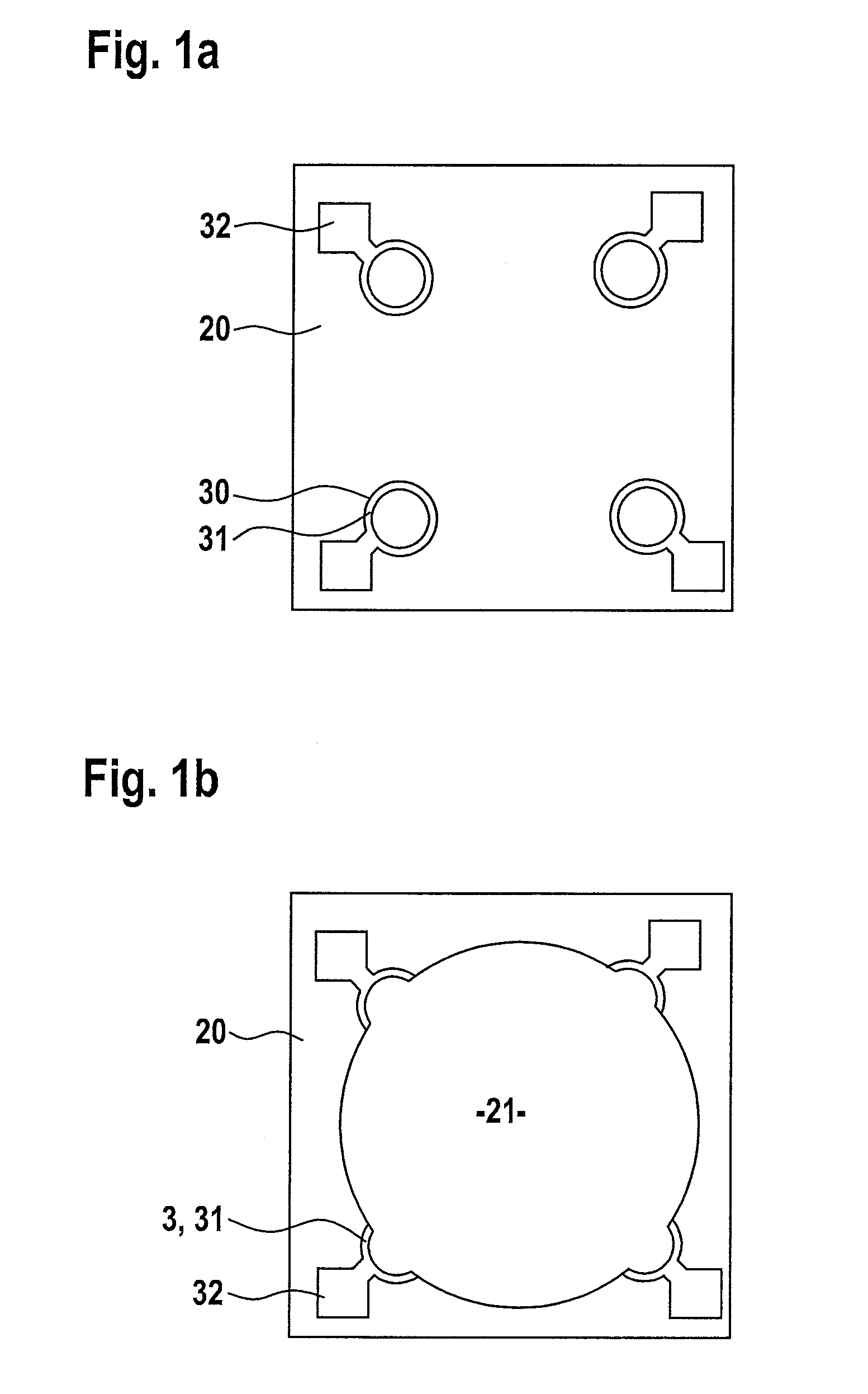
[0029]This support functions on the one hand as an interposer in the second-level mounting of the MEMS component. As such, the support is provided with at least one electrical feedthrough which establishes an electrical connection between the MEMS component on the front side of the support and further wiring planes within or on the rear side of the support.

[0030]On the other hand, the support at least laterally delimits a cavity adjoining the diaphragm structure of the MEMS component. In the microphone components described below, this cavity is used as the rear side volume.

[0031]The component design based on the packaging concept according to the present invention is depicted with reference to the section of a microphone component 100 sch...


PUM

PropertyMeasurementUnit
electrically conductiveaaaaaaaaaa
surface areaaaaaaaaaaa
front volumeaaaaaaaaaa

Abstract

A packaging concept for MEMS components having at least one diaphragm structure formed in the front side of the component is provided, according to which the MEMS component is mounted on a support which at least laterally delimits a cavity adjoining the diaphragm structure. In addition, at least one electrical feedthrough is formed in the support which allows electrical contacting of the MEMS component through the support. To achieve the largest possible rear volume for the diaphragm structure of the MEMS component for a given chip surface area, and also to simplify the processing of the support, according to the invention the electrical feedthroughs are integrated into the wall of the cavity adjoining the diaphragm structure, in that at least one section of such a feedthrough is implemented in the form of an electrically conductive coating of a side wall section of the cavity.

Description

RELATED APPLICATION INFORMATION[0001]The present application claims priority to and the benefit of German patent application no. 10 2012 220 323.0, which was filed in Germany on Nov. 8, 2012, the disclosure of which is incorporated herein by reference.FIELD OF THE INVENTION[0002]The present invention relates to the packaging of microelectromechanical system (MEMS) components having a diaphragm structure formed in the front side of the component. The component may be a pressure sensor, a speaker, or a microphone component, for example.[0003]Such packaging is not only used for mechanical protection of the MEMS component, but also generally contributes significantly to the implementation and performance of the particular MEMS function. This is particularly apparent in the example of a microphone component. The sound opening of such a component is formed in the packaging of a MEMS microphone component, via which the front volume and a rear volume which is as large as possible are also i...

Claims


Application Information

Patent Timeline
Patent Type & Authority Patents(United States)
IPC IPC(8): B81B7/00B81C1/00H04R7/04H01L41/31H01L41/053B81B3/00H04R19/04
CPCB81B7/007B81B3/00B81B3/0021B81B3/0027B81B3/0032B81B7/0032B81B7/0058B81B7/0061B81C1/00158H01L41/053H01L41/0533H01L41/31H04R7/04H04R7/045H04R19/04B81B2201/0257B81B2207/092B81B2207/096H01L2224/20H01L2224/04105H10N30/07H10N30/88H10N30/883
Inventor ZOELLIN, JOCHENEHRENPFORDT, RICARDOSCHELLING, CHRISTOPHGRAF, JUERGENANTE, FREDERIKCURCIC, MICHAEL
Owner ROBERT BOSCH GMBH
Why Eureka
Try Eureka