Dielectric laser electron accelerators

a dielectric laser and electron accelerator technology, applied in the direction of laser details, excitation process/apparatus, electric discharge tubes, etc., can solve the problems of increasing the difficulty of shrinking the rf electron accelerator to tabletop size for portable applications, increasing the difficulty of structure design, and bulky traditional rf electron accelerators, etc., to achieve simple fabrication process and improve accelerator performance.

Active Publication Date: 2015-12-15
THE BOARD OF TRUSTEES OF THE LELAND STANFORD JUNIOR UNIV
View PDF23 Cites 3 Cited by
  • Summary
  • Abstract
  • Description
  • Claims
  • Application Information

AI Technical Summary

Benefits of technology

[0007]The present invention provides, in one aspect, high-performance, compact and cost-effective integrated accelerator structures for tunable electron beam based light sources. Advantageously, embodiments of the present invention use structures such that the laser pulses are orthogonal to the electron beams, so phase velocity matching is less of a concern. In embodiments of the invention, accelerator structures are designed based on buried gratings and photonic crystals. Asymmetric structures and random structures may be used to optimize the accelerating fields. The performance of the devices may be improved using a material coating and hydrogen annealing.
[0009]These accelerator structures can be fabricated using CMOS and MEMS compatible materials and processes, thus leveraging the well-developed CMOS and MEMS industry at low cost. Furthermore, the CMOS and MEMS compatible processes allow the structures and components to be integrated on a chip, which makes the devices well suited for portable light sources.
[0012]A compact laser-driven dielectric electron accelerator according to embodiments of the present invention may be use to implement tunable electron based light sources. The device provides improved accelerator performance with simple fabrication process, thus is well-suited for various applications. For example, this device can be used as a light source for oil well jogging, especially used as a miniaturized version of the live fluid analyzer. This device can also be used in medical applications such as medical diagnostics, radiation therapy for cancer, and medical imaging. Other applications include mass spectrometry, ion implantation, and X-ray microlithography.

Problems solved by technology

Traditional RF electron accelerators are bulky.
These physical limitations increase the difficulty of shrinking RF electron accelerators to tabletop sizes for portable applications.
This increases difficulties in structure design (to match the phase velocity), coupler design (to couple light into structure efficiently) and integration between accelerators and other components.

Method used


Image

  • Dielectric laser electron accelerators
  • Dielectric laser electron accelerators
  • Dielectric laser electron accelerators

Examples


Embodiment Construction

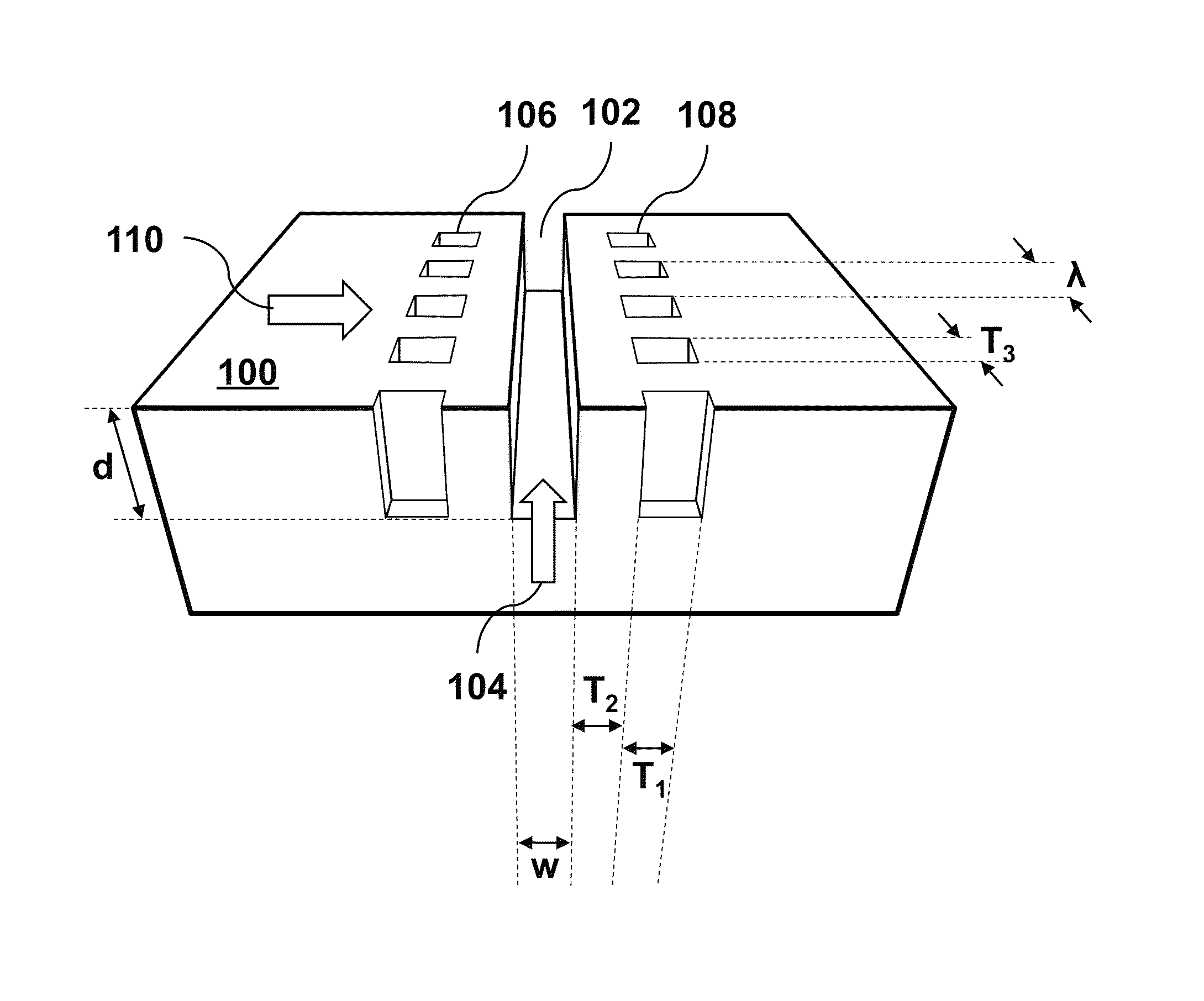
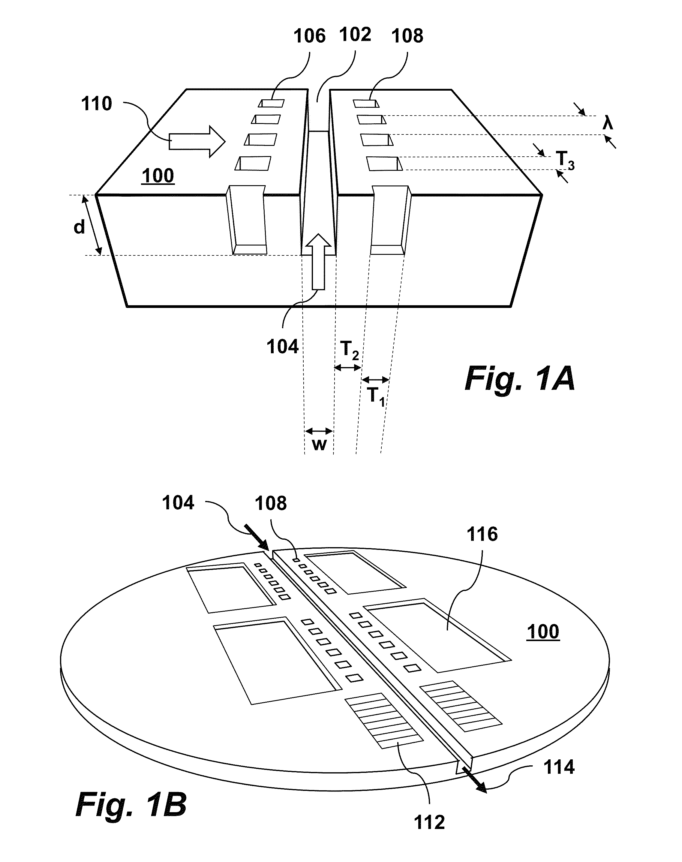
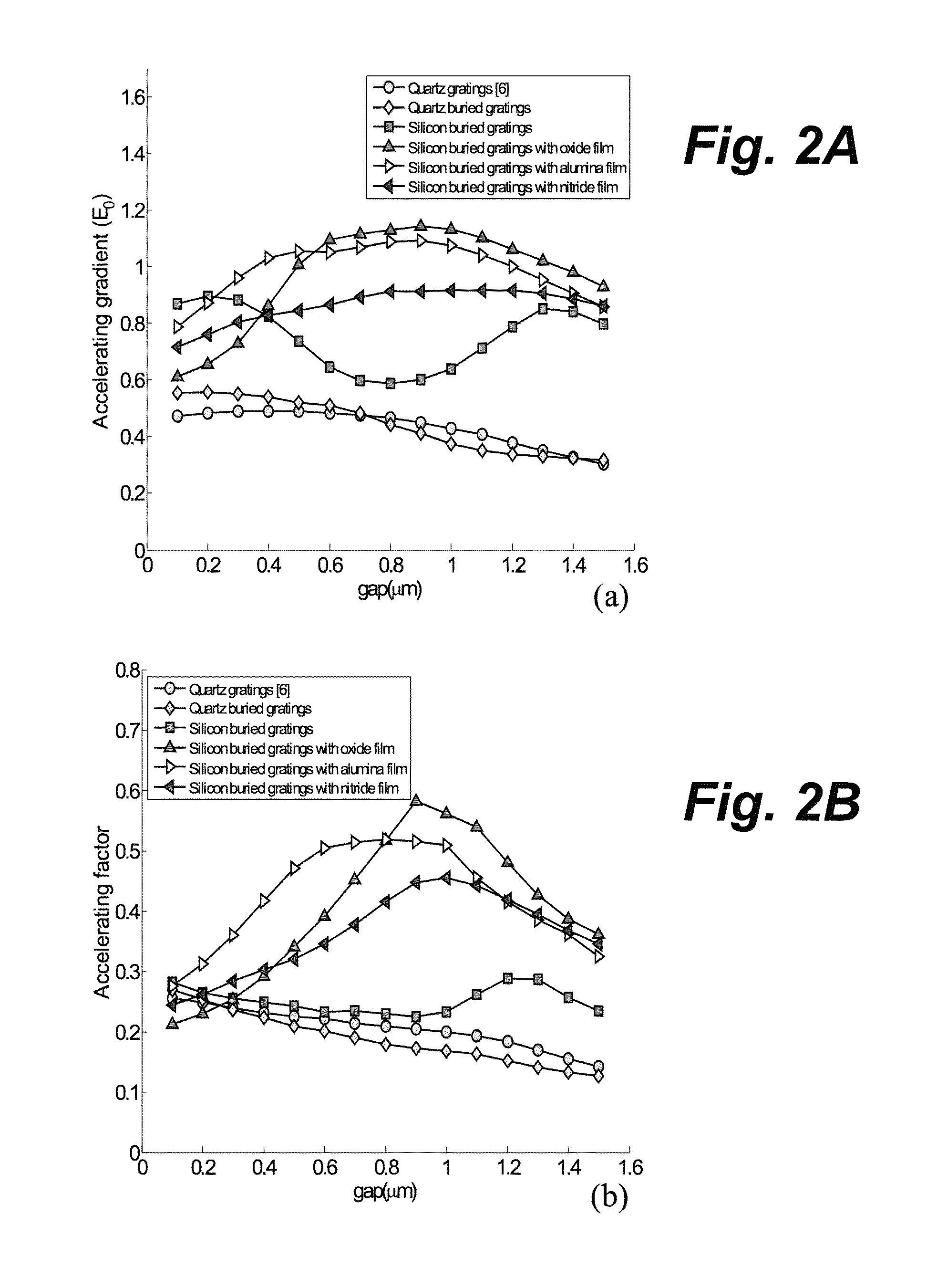
[0018]Laser-driven dielectric electron accelerators have been studied since first being proposed in 1962. The use of high power lasers and dielectric materials has the potential to increase the accelerating gradients to GV / m, enabling miniaturization of accelerators for ultra-compact portable light sources. However, laser-driven, miniaturized accelerators have not yet been realized due to the lack of practical accelerator designs and manufacturing processes. With recent advances in ultrashort pulse lasers and semiconductor technology, however, electron accelerators with chip-scale dimensions have become possible. This has heightened the need for accelerator designs that can efficiently transfer laser energy to electron energy.

[0019]Prior designs have included guided structures, such as photonic crystal holey fibers, and optical Bragg structures. In these structures, the electron beam is co-propagating with the laser beam so that the electron beam can be accelerated by the longitudin...


PUM


Abstract

A laser-driven dielectric electron accelerator is composed of a dielectric photonic crystal accelerator structure having an electron beam channel and buried grating whose elements are arranged linearly parallel to the electron beam channel. The accelerator structure preferably has a thin film material coating. The grating may have an asymmetric structure. The accelerator and undulator structures may be integrated with on-chip optical and electronic devices such as waveguide devices and control circuits so that multiple devices can be fabricated on the same chip.

Description

CROSS-REFERENCE TO RELATED APPLICATIONS[0001]This application claims priority from U.S. Provisional Patent Application 61 / 699,398 filed Sep. 11, 2012, which is incorporated herein by reference.STATEMENT OF GOVERNMENT SPONSORED SUPPORT[0002]This invention was made with Government support under contract N66001-11-1-4199 awarded by Space and Naval Warfare Systems Command. The Government has certain rights in this invention.FIELD OF THE INVENTION[0003]This invention relates generally to improved dielectric laser electron accelerators.BACKGROUND OF THE INVENTION[0004]Traditional RF electron accelerators are bulky. The transverse size of the RF electron accelerator is about four orders of magnitude larger than that of the optical electron accelerator. Traditional RF electron accelerators are also limited by smaller accelerator gradient (˜30 MV / m), compared to the optical electron accelerators (>1 GV / m). As a result, the accelerator length of the traditional RF electron accelerator is a...

Claims


Application Information

Patent Timeline
Patent Type & Authority Patents(United States)
IPC IPC(8): H01J23/00H01S3/09H05H7/04H05H15/00
CPCH05H15/00H01S3/0903H05H7/04H05H2007/041
Inventor SOLGAARD, OLAVCHANG, CHIA MING
Owner THE BOARD OF TRUSTEES OF THE LELAND STANFORD JUNIOR UNIV
Why Eureka
Try Eureka