Multi-magnification high sensitivity optical system for probing electronic devices

a high-sensitivity, optical system technology, applied in the field of multi-magnification high-sensitivity optical systems for probing electronic devices, can solve the problems of reducing the yield of these devices, increasing manufacturing costs, and emerging new causes of yield decline, and achieves high resolution and easy mounting and switching.

Active Publication Date: 2015-12-22
CHECKPOINT TECH
View PDF10 Cites 6 Cited by
  • Summary
  • Abstract
  • Description
  • Claims
  • Application Information

AI Technical Summary

Benefits of technology

[0006]The present application discloses a multi-resolution microscopy system for testing and probing semiconductor integrated circuits. Optical probes at different magnifications can be easily mounted and switched, allowing measurement with high resolution through high N.A. solid immersion lenses. The presently disclosed optical probe system provides a rotational stage that can hold multiple optical objective systems at different magnifications and provides full positional and tilt adjustment capabilities to each optical objective system. A magnetic sensing system can detect the positions of the optical objective systems. The magnetic sensing system does not generate light that can affect the highly sensitive optical measurement of the optical probe. The rotational stage is further equipped with mechanism to bypass water and prevent it from damaging electronics under the rotational stage. A flexible circuit is configured to transmit electronic signals from the processors and controllers in the fixed frame to the optical objective system that can rotate on the rotational stage.
[0007]The optical measurement in the presently disclosed optical probe system is isolated from mechanical disturbances in the surrounding environment, which reduces or eliminates measurement errors caused by mechanical vibrations. The optical measurement is isolated from vibration induced by coolant being injected onto the IC under test, which reduces or eliminates measurement errors caused by the interference of the flowing coolant with the optical focus and axis. The disclosed system and method provide proper cooling to remove heat generated during the optical measurement. The disclosed system and method can also provide heating to simulate harsh operating conditions to the device under test. Thermal control fluid is sealed and kept in the temperature control chamber by a reliable vacuum seal. The vacuum seal itself is compatible with multiple objectives provided they conform to the proper geometry. The seal includes a flexible portion and allows the optical probe to be accurately positioned to different locations on the target IC. The temperature control chamber is mounted in such a manner that it allows for vibration isolation from the chamber; it allows the IC under test to be tipped and tilted with respect to the optical axis; and it allows for precise placement of the optical axis onto the IC. The temperature control chamber mount is capable of centering the chamber at a different point than the optical axis, this is controlled by the design of the chamber mount and a movement scheme implemented via the computer control.

Problems solved by technology

The cost of manufacturing has increased and the yield has decreased for these devices.
New causes of yield decrease emerge as different materials are utilized and the process variation tolerances shrink.
The decreasing sizes of circuit features in electronic devices create a significant challenge for probe tools.
Another challenge for the probing systems is to suppress measurement errors caused by mechanical disturbances.
Moreover, a significant amount of heat can be generated by operating the device at design speeds and voltages during optical measurements, and the light source from the probing tool can also generate heat when focused onto an IC device, both of which can affect the proper function of the integrated circuit.
As such another challenge for probing systems is to remove the increasing amount of heat generated during the debug and test procedures.

Method used


Image

  • Multi-magnification high sensitivity optical system for probing electronic devices
  • Multi-magnification high sensitivity optical system for probing electronic devices
  • Multi-magnification high sensitivity optical system for probing electronic devices

Examples


Embodiment Construction

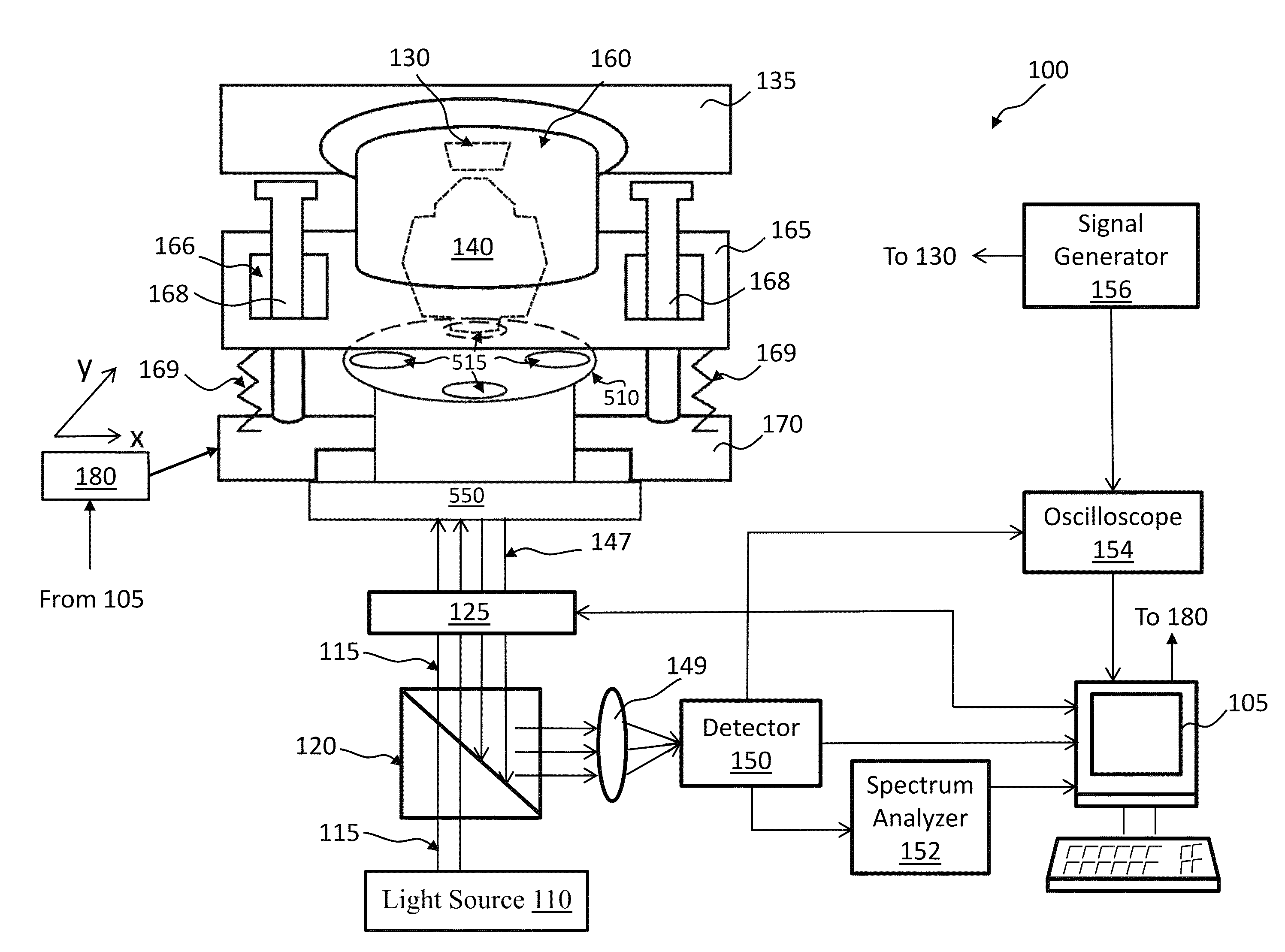
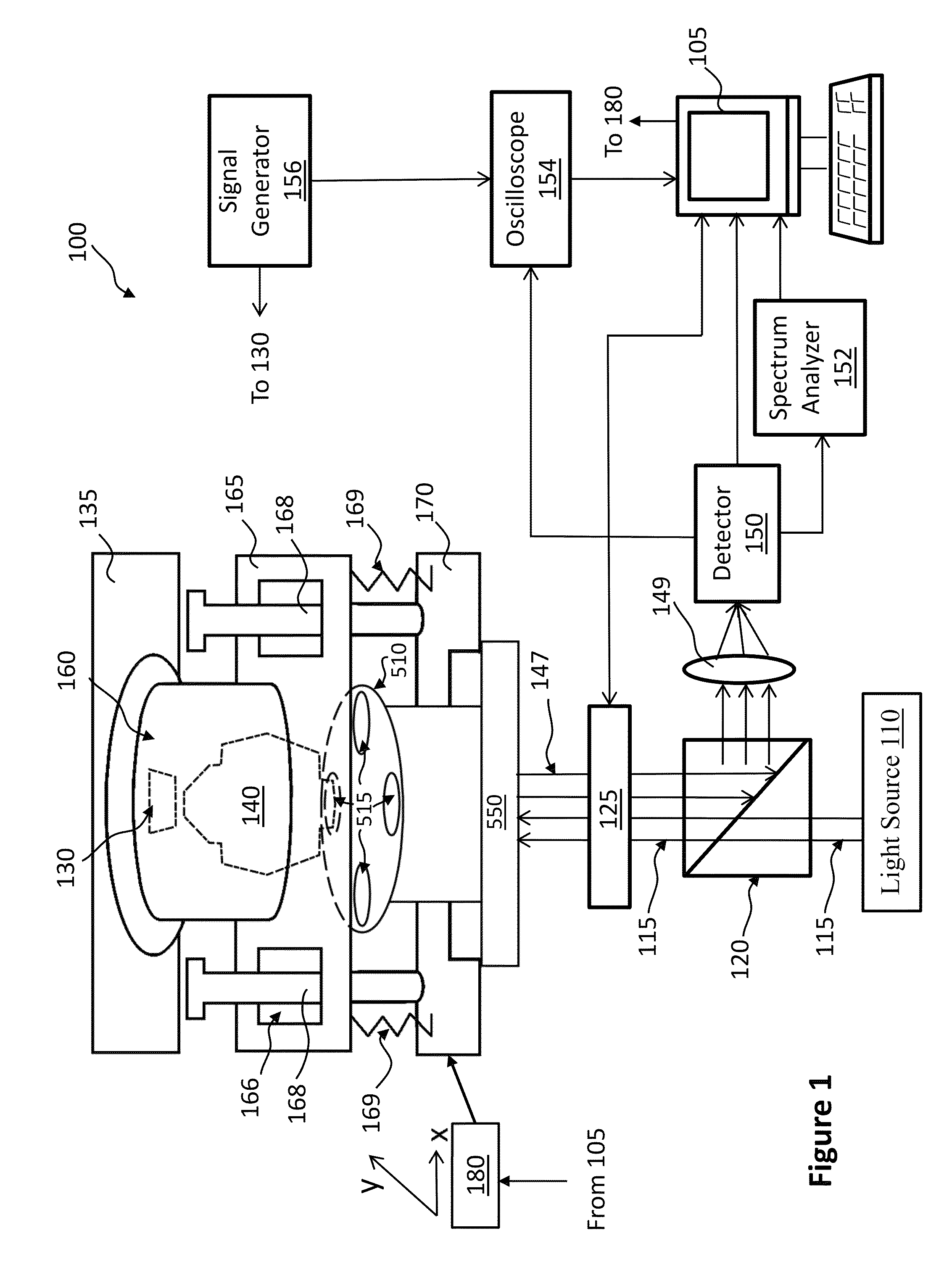
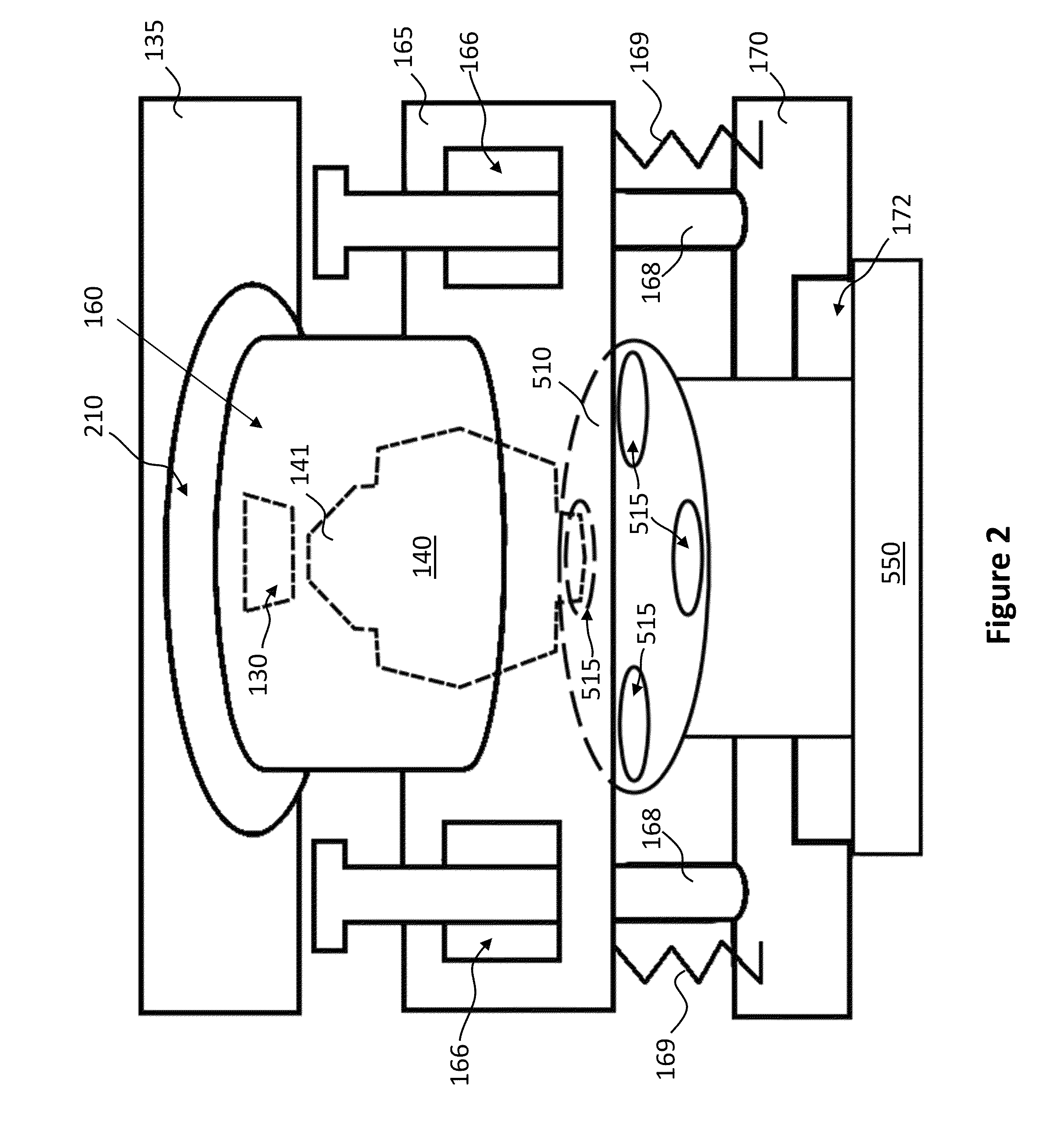
[0026]Referring to FIGS. 1 and 2, an optical probe system 100 includes a light source 110, a beam splitter 120, a scanning system 125, an optical objective system 140, a photo detector 150, a spectrum analyzer 152, an oscilloscope 154, a signal generator 156, and a computer 105. The light source 110 can be implemented by a laser emitting device (such as tunable or continuous wave (CW) laser source or other light sources such as a pulsed or mode-locked laser), or a non-coherent light source. Incident light 115 emitted by the light source 110 passes the beam splitter 120. The photo detector 150 can be implemented by an avalanche photo detector. The scanning system 125 can be implemented by moveable galvo mirrors which can also include Acoustic-Optics Device, deflector scanning lens, and tube lens etc. As described in more detail below, the optical objective system 140 is mounted in one of several ports 515 in a rotational stage 510. The rotational stage 510 can hold, in the several po...


PUM


Abstract

An optical probe system for probing an electronic device includes a sample plate configured to hold a target device comprising an integrated circuit, a temperature control chamber configured to hold a fluid to control the temperature of the target device, a first optical objective system that can collect reflected or emitted light from the integrated circuit in the target device, a rotational stage including ports that can hold the optical objective systems, a vertical translation stage that can move the first optical objective system in a vertical direction substantially perpendicular to the sample plate, and an x-y translation stage that can move the first optical objective system in horizontal directions. A portion of the first optical objective system is moved through the temperature control chamber to allow the first optical objective system to focus at the target device.

Description

BACKGROUND OF THE INVENTION[0001]The present application relates to systems and methods for probing features and functions of semiconductor integrated circuits (ICs).[0002]To improve IC functionality and performance, IC manufacturers in the last four decades have been shrinking the sizes of circuit components, and at the same time, increasing the number of circuit components per IC. As electronic devices become more miniaturized and more powerful, IC devices become smaller and more devices are packed onto each chip. The cost of manufacturing has increased and the yield has decreased for these devices. New causes of yield decrease emerge as different materials are utilized and the process variation tolerances shrink.[0003]Probe tools are frequently utilized during the testing and debugging of IC designs, where efforts are focused on defect localization and accurate waveform and timing measurements of signal switching inside silicon-based devices. Both signal measurements and optical ...

Claims


Application Information

Patent Timeline
Patent Type & Authority Patents(United States)
IPC IPC(8): G02B21/00
CPCG02B21/0016G02B21/248G02B21/26
Inventor CLAWGES, THOMAS EMORGAN, DAVID JXIAO, GUOQING
Owner CHECKPOINT TECH
Why Eureka
Try Eureka