Package and manufacturing method of the same

a manufacturing method and packaging technology, applied in the direction of printed circuit details, solid-state devices, metal pattern materials, etc., can solve the problems of shortening the manufacturing period, shortening the process time and high material cost of substrate production, and reducing the production efficiency of substrates. , to achieve the effect of shortening the material and process time, shortening the manufacturing period, and enhancing the attachment strength

Active Publication Date: 2015-12-22
SUZHOU LEKIN SEMICON CO LTD
View PDF104 Cites 0 Cited by
  • Summary
  • Abstract
  • Description
  • Claims
  • Application Information

AI Technical Summary

Benefits of technology

[0019]According to the embodiments of the present invention, a substrate may be formed by printing or coating a paste- or ink-type insulator and conductor on a patterned layer that is formed on a sapphire wafer. Thus, no void is created between the substrate and LED chip, thus enhancing attachment strength.
[0020]Further, since the insulator containing a ceramic component is cured at a low temperature, it may be possible to minimize contraction of the wafer that occurs when the ceramics is fired and resultant damage to the wafer. And, problems with co-planarity of substrate that are issued in the existing wafer-to-wafer bonding process may be solved thanks to a printing method utilizing paste or ink with viscosity.
[0021]Moreover, the package is produced by a printing method instead of the existing substrate manufacturing process and substrate attachment process and thus several steps may be unnecessary. Accordingly, it may be possible to shorten costs of material and process and manufacturing period. Further, the phosphor or ESD protection material contained in the insulator may enhance luminous efficiency or provide an antistatic feature.

Problems solved by technology

Such a void may weaken attachment strength.
In the conventional LED package and the method of manufacturing the LED package, the Si substrate has excellent flatness compared to other substrates, but has disadvantages of a long process time and a high material cost for substrate production.
The ceramic substrate, such as AlN or LTCC substrate, has a lower material cost than that of other substrates, but has a relatively long process time and poor flatness.
Further, as described above, there is a problem that a void occurs between the chip and the insulating layer.

Method used


Image

  • Package and manufacturing method of the same
  • Package and manufacturing method of the same
  • Package and manufacturing method of the same

Examples


Embodiment Construction

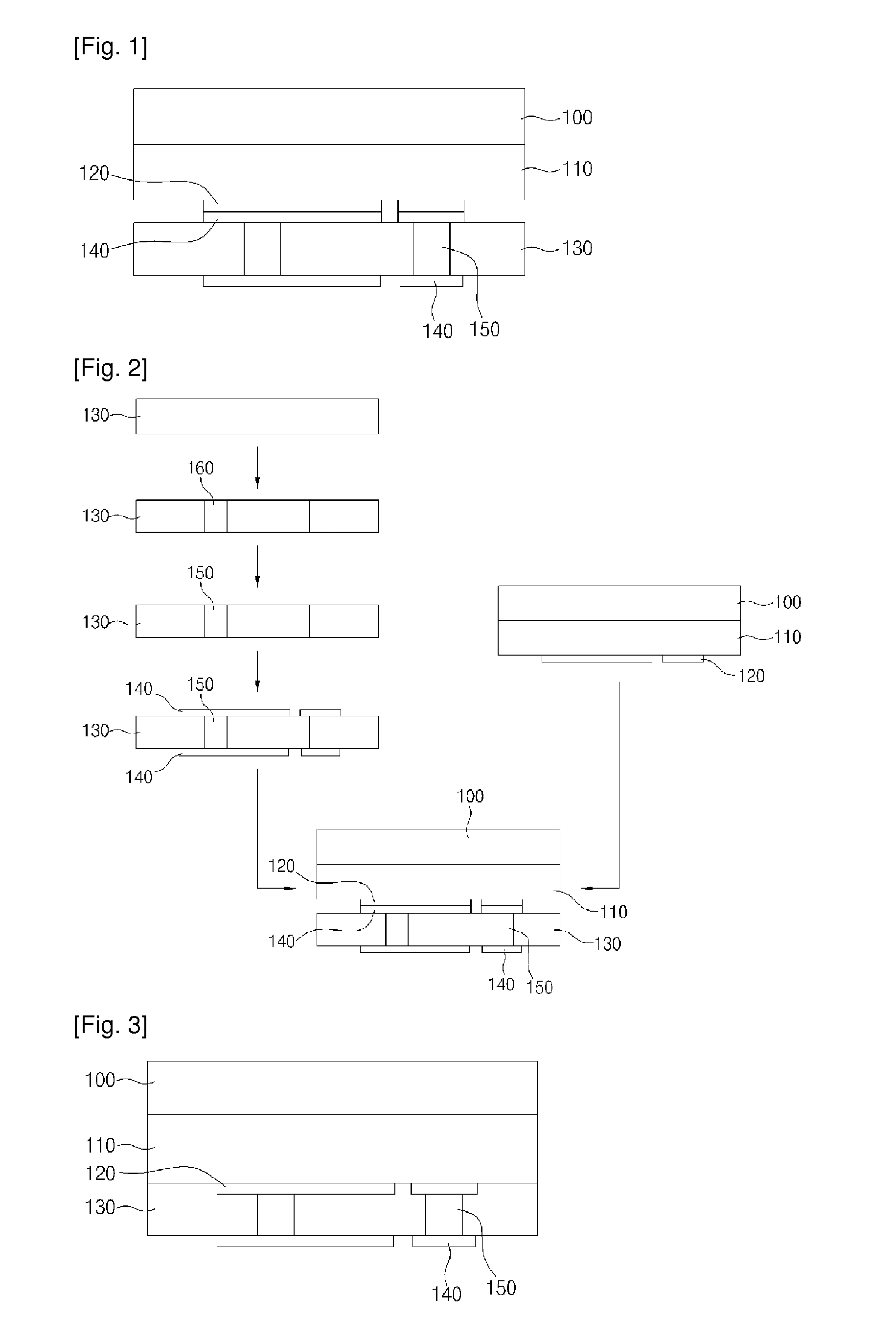
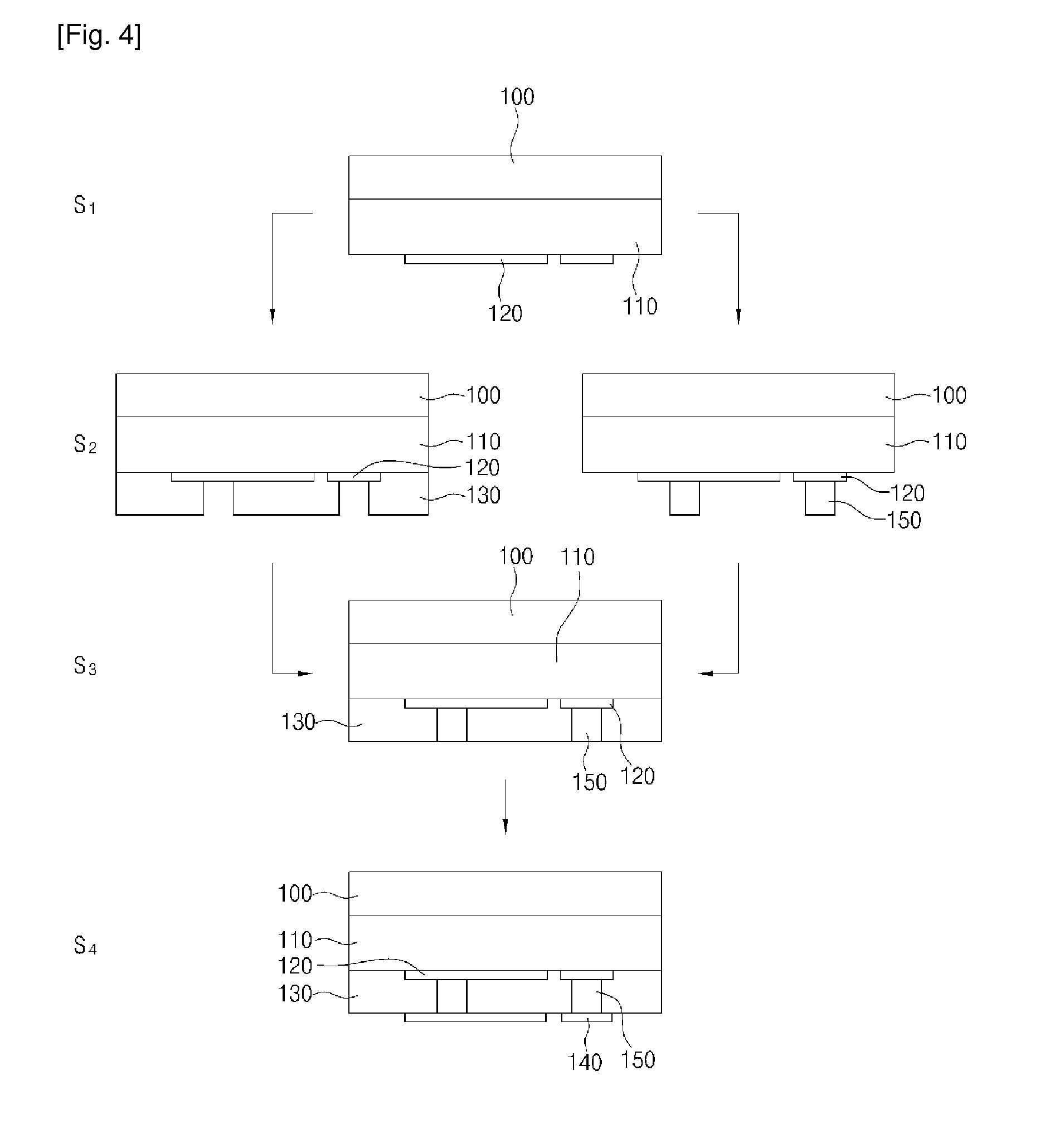
[0026]Hereinafter, a package and a method of manufacturing the package according to an embodiment of the present invention will be described in greater detail with reference to the accompanying drawings. The related well known functions or constructions that are determined to make the gist of the invention unnecessarily unclear will be excluded from the description of the embodiment. In the drawings, the sizes of the elements may be exaggerated for clarity.

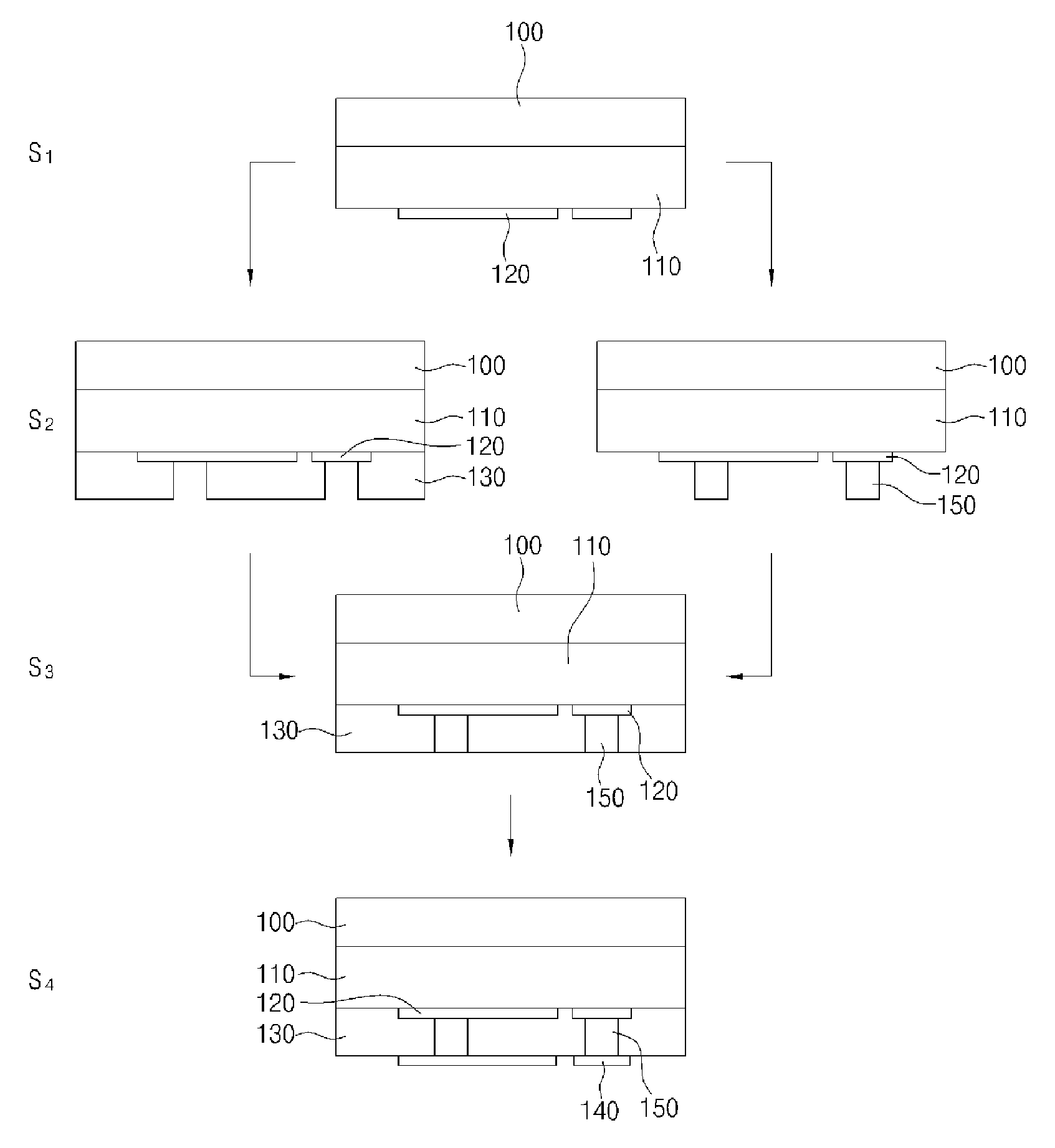
[0027]FIG. 3 is a cross sectional view illustrating a package according to an embodiment of the present invention. Referring to FIG. 3, the package includes a sapphire substrate 100, a (LED or semiconductor) patterned layer 110, a first conductive layer 120, an insulating layer 130, a second conductive layer 140, and a third conductive layer 150. Specifically, an LED chip includes the patterned layer 110 and the first conductive layer 120 sequentially formed under the sapphire substrate 100. The insulating layer 130 is formed unde...


PUM

PropertyMeasurementUnit
particle sizeaaaaaaaaaa
temperatureaaaaaaaaaa
conductiveaaaaaaaaaa

Abstract

Provided are a package including a first conductive layer on a patterned layer, an insulating layer on the patterned layer burying the first conductive layer, a second conductive layer on an outer surface of the insulating layer, and a third conductive layer in the insulating layer electrically connecting the first conductive layer with the second conductive layer. A substrate is formed by printing or coating a paste- or ink-type insulator and conductor on a patterned layer formed on a sapphire wafer. No void is created between the substrate and LED chip, thus enhancing attachment strength. The ceramic-containing insulator is cured at a low temperature, thereby minimizing contraction of and damage to the wafer when the ceramic is fired. Printing methods utilizing viscous paste or ink solves problems with co-planarity of substrate that occur in existing wafer-to-wafer bonding processes and renders several steps of the existing substrate manufacturing process unnecessary.

Description

CROSS-REFERENCE TO RELATED APPLICATIONS[0001]This application is the U.S. national stage application of International Patent Application No. PCT / KR2010 / 009288, filed Dec. 23, 2010, which claims priority to Korean Patent Application Nos. 10-2010-0004797, filed Jan. 19, 2010, and 10-2010-0023923, filed Mar. 17, 2010, the disclosures of each of which are incorporated herein by reference in their entirety.TECHNICAL FIELD[0002]The present disclosure is directed to a package and a method of manufacturing the package. More specifically, the present disclosure is directed to a package that may enhance attachment capability since there is no void between a chip and an insulating layer and a method of manufacturing the package.BACKGROUND ART[0003]Light emitting diodes (“LEDs”) emit light when forward biased. LEDs employ field effects as a light emitting principle. LEDs have an even longer life span than that of incandescent lamps. LEDs may emit various colors of light from ultraviolet rays th...

Claims


Application Information

Patent Timeline
Patent Type & Authority Patents(United States)
IPC IPC(8): H05K1/03H01L33/62H01L33/44H01L33/00
CPCH01L33/62H01L33/0079H01L33/44H01L2924/0002H01L2933/0066H01L2924/00H01L33/486H01L33/0093
Inventor HAN, YOUNG JUHWANG, DEOK KILIM, JAE CHUNG
Owner SUZHOU LEKIN SEMICON CO LTD
Why Eureka
Try Eureka