Method for manufacturing MTJ memory device

a technology of memory device and mtj, which is applied in the direction of magnetic field-controlled resistors, semiconductor devices, galvano-magnetic material selection, etc., can solve the problems of reducing the efficiency of mtj devices. , to achieve the effect of reducing damage and reducing material re-deposition

Active Publication Date: 2016-02-16
INTEGRATED SILICON SOLUTION CAYMAN INC
View PDF174 Cites 94 Cited by
  • Summary
  • Abstract
  • Description
  • Claims
  • Application Information

AI Technical Summary

Benefits of technology

[0010]The disclosed method solves the problem of conventional MTJ device manufacturing by reducing the re-deposition of material on the sides of the MTJ pillar, preventing shunts from being formed at the edges of the tunnel barrier layer, and reducing damage caused at the edges of the MTJ layers by using high angle ion beam cleaning.
[0011]Through the use of discrete ion beam etching steps, the manufacturing method disclosed herein limits or eliminates the need for high angle ion beam cleaning, provides a processing method that solves one of the biggest manufacturing hurdles with MTJ MRAM technology—processing of high density or closely spaced MTJ pillars—and enables the use of current process tooling / technology to define the MTJ pillars.

Problems solved by technology

However, under conventional manufacturing schemes, forming pillar like MTJ devices without shunts and at a DRAM-like density is not manufacturable.
One limitation of the current processing technology is illustrated in FIG. 1.
As a result, their presence at the edges 122 of the barrier layer of the MTJ pillar 120 is significantly detrimental to the operation of the device.
However, this removal process puts unacceptable limits on the device density.
Furthermore, sidewall cleaning at high ion beam angles significantly increases the beam damage to the thin MTJ layers, which only further compromises the MTJ performance.
Although the MRAM development companies have spent significant resources and effort to develop ion beam cleaning techniques as well as other manufacturing processes, such as reactive ion etching, the existing manufacturing processes have not lead to a satisfactory process and tooling technology for MTJ pillars.

Method used


Image

  • Method for manufacturing MTJ memory device
  • Method for manufacturing MTJ memory device
  • Method for manufacturing MTJ memory device

Examples


first embodiment

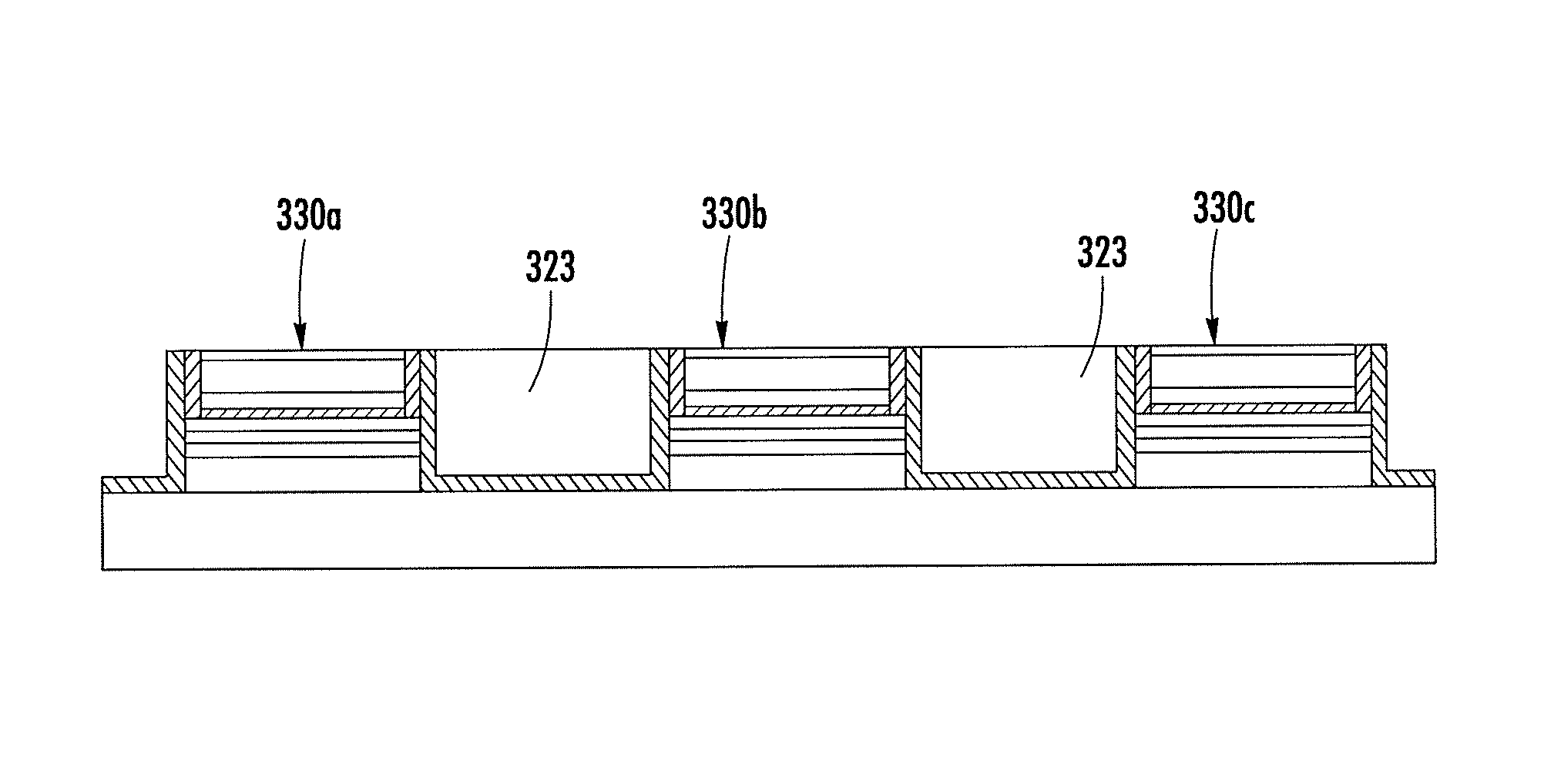
[0026]FIGS. 5A and 5B-5D illustrate two alternative embodiments for etching the MTJ layer stack to the barrier layer 315 of the MTJ structure. In particular, FIG. 5A illustrates the etching step. As shown, the etching step result in formation of MTJ pillar 330 having a width defined by the width of photoresist 319. As noted above, in the exemplary embodiment, the barrier layer 315 is formed from an oxide of magnesium (MgO). It should be appreciated that processing of MTJ layer stack into MTJ pillar shaped devices requires precise control of the etching depth through all of the stack layers. The barrier resistance control is partially determined based on precision of the etching on the free layer 316 and the barrier layer 315. To eliminate shunting and to reduce the free layer 316 edge damage, stopping at the barrier layer 315 across the wafer is necessary to eliminate the re-deposition on the barrier layer 315. Furthermore, it should be appreciated that stopping at the barrier layer...

second embodiment

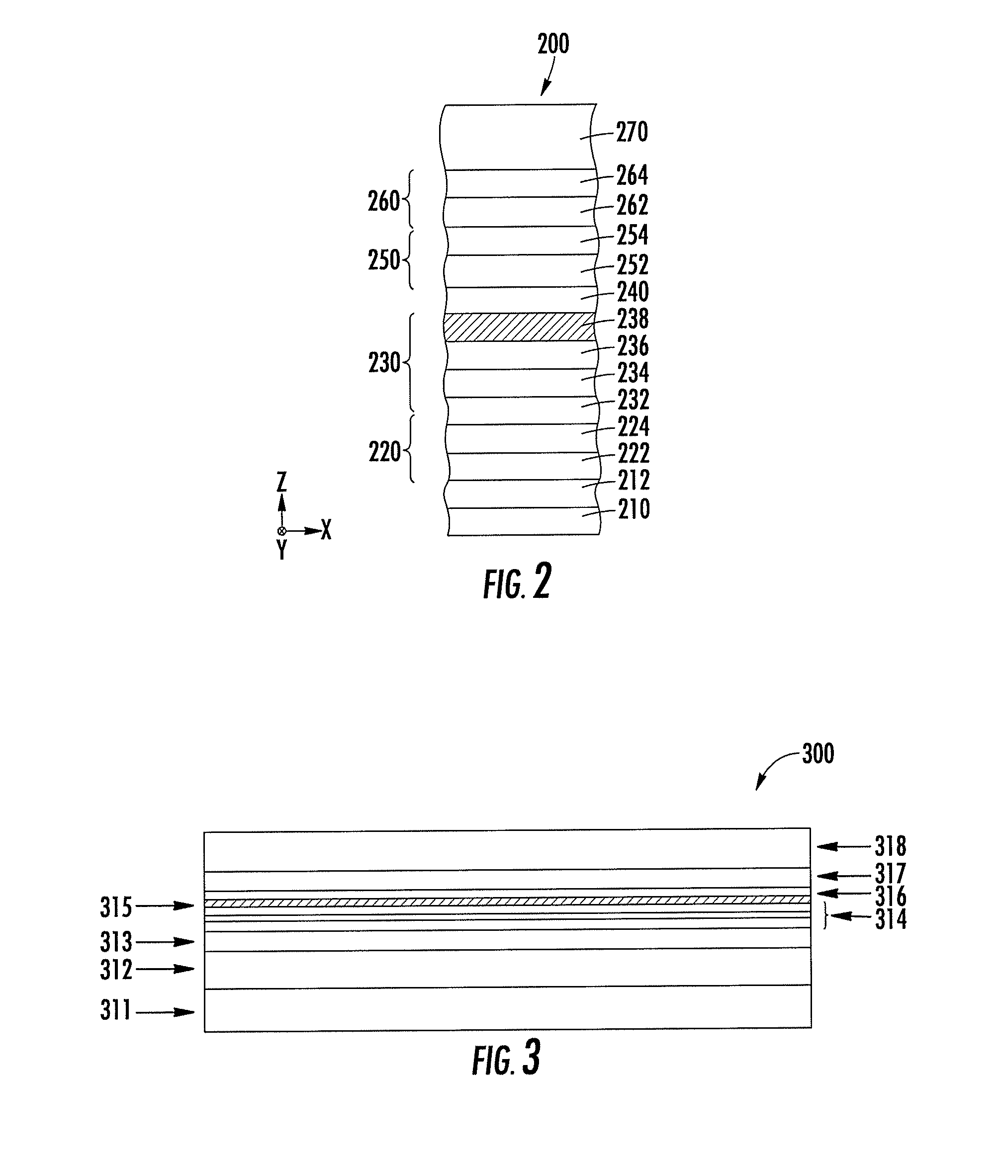
[0028]FIGS. 5B-5D illustrate a second embodiment for etching the MTJ layer stack according to the exemplary embodiment. In particular, FIGS. 5B-5D illustrate etching using multiple ion beam etching and reactive ion etching techniques (both shown in FIG. 5B-5D as downward facing arrows for illustrative purposes). First, after photoresist 319 is applied as shown in FIG. 4, the hard mask 318 is etched using reactive ion etching and the upper layers 317, including perpendicular polarizer 250, down to TaN capping layer 238 (which is illustrated as part of upper layers 317) are etched using ion beam etching. These two etching steps are collectively shown in FIG. 5B.

[0029]It should be appreciated that similar manufacturing methods for MTJ pillars have not been developed for layer stacks having perpendicular polarizers 250 and the like. Therefore, conventional manufacturing methods do not contemplate a separate ion beam etching after the photoresist 319 has been etched using reactive ion et...


PUM


Abstract

A method for manufacturing MTJ pillars for a MTJ memory device. The method includes depositing multiple MTJ layers on a substrate, depositing a hard mask on the substrate and coating a photoresist on the hard mask. Further, alternating steps of reactive ion etching and ion beam etching are performed to isolate MTJ pillars and expose side surfaces of the MTJ layers. An insulating layer is the applied to protect the side surfaces of the MTJ layers. A second insulating layer is deposited before the device is planarized using chemical mechanical polishing.

Description

BACKGROUND[0001]1. Field[0002]The present patent document relates generally to a method for manufacturing MRAM devices, and, more particularly, to a method for manufacturing MTJ pillars for MTJ memory devices with improved density and quality specifications.[0003]2. Description of the Related Art[0004]Magnetoresistive random-access memory (“MRAM”) is a non-volatile memory technology that stores data through magnetic storage elements. These elements are two ferromagnetic plates or electrodes that can hold a magnetic field and are separated by a non-magnetic material (i.e., a barrier layer), such as a non-magnetic metal or insulator. In general, one of the plates has its magnetization pinned (i.e., a “reference layer”), meaning that this layer has a higher coercivity than the other layer and requires a larger magnetic field or spin-polarized current to change the orientation of its magnetization. The second plate is typically referred to as the free layer and its magnetization directi...

Claims


Application Information

Patent Timeline
Patent Type & Authority Patents(United States)
IPC IPC(8): H01L29/82H01L43/12H01L43/10H01L43/02H01L43/08
CPCH01L43/12H01L43/02H01L43/08H01L43/10H10N50/10H10N50/01H10N50/80H10N50/85
Inventor PINARBASI, MUSTAFA
Owner INTEGRATED SILICON SOLUTION CAYMAN INC
Why Eureka
Try Eureka