Optical device, detection apparatus, electronic apparatus, and method for producing optical device

a detection apparatus and optical technology, applied in the field of optical devices, can solve problems such as difficulty in forming the capture space, and achieve the effect of improving the detection sensitivity

Inactive Publication Date: 2016-04-26
SEIKO EPSON CORP
View PDF6 Cites 2 Cited by
  • Summary
  • Abstract
  • Description
  • Claims
  • Application Information

AI Technical Summary

Benefits of technology

[0013]An advantage of some aspects of the invention is to provide an optical device, a detection apparatus, an electronic apparatus, and a method for producing an optical device, capable of further improving the detection sensitivity by capturing a substance such as a target molecule in a capture space formed by at least two types of organic molecules.
[0014]An advantage of some other aspects of the invention is to provide an optical device, a detection apparatus, an electronic apparatus, and a method for producing an optical device, capable of further improving the detection sensitivity by regularly arranging a capture space matched with the size of a substance such as a target molecule.
[0020]The capture region having a depth corresponding to the chain length difference between the first organic group and the second organic group and having a width corresponding to the arrangement interval of the first organic molecule having a longer chain length between the first and the second organic molecules is regularly formed. Therefore, the density of the capture region in which a given substance, for example, a target molecule can be held by multipoint adsorption is increased, and a detection signal level for the target molecule or the like can be increased.
[0022]According to this configuration, the length A1 of one of the axes defining the maximum projected area of a given substance, for example, a target molecule falls within the width w of the capture region, and the length A2 of the other of the axes defining the maximum projected area of the target molecule falls within the depth r of the capture region, and thus, the target molecule can be adsorbed in the capture region conforming to the size of the target molecule. In particular, in the case where A1<A2, the target molecule can fit in the width w of the capture region in a vertically long state. As a result, it becomes possible to select the target molecule by the capture region. That is, a noise molecule having a size larger than the target molecule is not captured in the capture region. In this manner, since the capture region is not occupied by a noise molecule, the detection signal level for the target molecule can be increased. Further, since the size of the capture region is not excessively increased, the density of the capture region is further increased.
[0024]According to this configuration, the length A1 of one of the axes defining the maximum projected area of a given substance, for example, a target molecule falls within the depth r of the capture region in a horizontally long state, and the length A2 of the other of the axes defining the maximum projected area of the target molecule falls within the width w of the capture region, and thus, the target molecule can be adsorbed in the capture region conforming to the size of the target molecule. Also in this case, in the same manner as (3), the detection signal level for the target molecule can be increased. However, the density of the capture region is lower than in the case of (3).
[0027](7) Another aspect of the invention relates to a detection apparatus including: a light source; the optical device according to any of the above (1) to (6), on which a light from the light source is incident; and a light detector which detects a light emitted from the optical device. The detection sensitivity of this detection apparatus is improved by using the above-described optical device.

Problems solved by technology

However, the above-described methods have a problem, for example, the same type of SAM molecules aggregate, or an SAM which is easily formed is preferentially formed, and therefore, it is difficult to form the capture space 212 in a regularly arranged pattern as shown in FIG. 2.

Method used


Image

  • Optical device, detection apparatus, electronic apparatus, and method for producing optical device
  • Optical device, detection apparatus, electronic apparatus, and method for producing optical device
  • Optical device, detection apparatus, electronic apparatus, and method for producing optical device

Examples


Embodiment Construction

[0065]Hereinafter, preferred embodiments of the invention will be described in detail. The embodiments described below do not unduly limit the contents of the invention described in the appended claims, and all of the structures described in the embodiments are not indispensable for the solving means of the invention.

1. Basic Structure of Optical Device

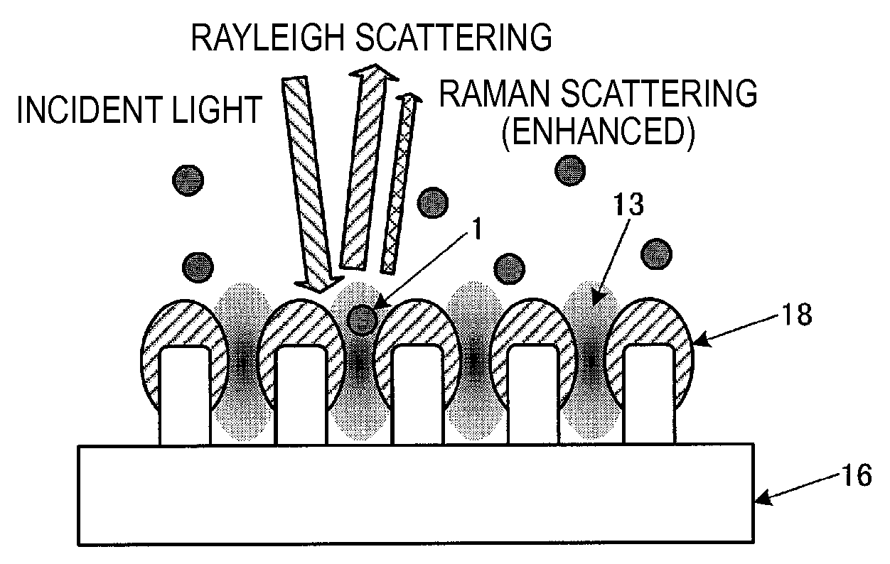
[0066]Optical devices 10 shown in FIGS. 3A to 3C each have a dielectric layer 16 on one outermost surface of a substrate 12. The substrate 12 itself may be a dielectric body such as an oxide, and in such a case, the substrate 12 can be formed from glass, mica, SiO2, SnO2, GeO2, ZrO2, TiO2, Al2O3, PZT, or the like. On the substrate 12 made of a material other than a dielectric body, the above-described dielectric layer 16 may be formed. In this embodiment, for example, a metal (dielectric) layer 14 can be provided between the substrate 12 made of glass and the dielectric layer 16.

[0067]On the dielectric layer 16, a metal microstructure...


PUM

PropertyMeasurementUnit
particle diameteraaaaaaaaaa
thicknessaaaaaaaaaa
thicknessaaaaaaaaaa

Abstract

An optical device includes: a substrate having a dielectric layer and a plurality of metal particles; and an organic molecular layer formed by self-assembly on at least either the surface of the dielectric layer or the surfaces of the metal particles. In the organic molecular layer, a first organic molecule and a second organic molecule are alternately arranged in a first direction, and the chain length of an organic group of the first organic molecule and the chain length of an organic group of the second organic molecule are different from each other.

Description

BACKGROUND[0001]1. Technical Field[0002]The present invention relates to an optical device, a detection apparatus, an electronic apparatus, and a method for producing an optical device.[0003]2. Related Art[0004]Recently, the demand for a sensor chip to be used for medical diagnoses, tests for foods and beverages, etc. has been increasing, and the development of a highly sensitive and small sensor chip has been demanded. In order to respond to such a demand, various types of sensor chips such as electrochemical sensor chips have been studied. Among these, for the reasons that integration is possible, the cost is low, measurement can be performed in any environment, etc., sensor chips using a spectroscopic analysis utilizing surface plasmon resonance (SPR), particularly, surface-enhanced Raman scattering (SERS) have drawn increasing attention.[0005]Here, the term “surface plasmon” refers to an oscillation mode of an electron wave that is coupled to light depending on boundary conditio...

Claims


Application Information

Patent Timeline
Patent Type & Authority Patents(United States)
IPC IPC(8): G01N21/00B82Y15/00G01J1/42G01N21/65
CPCG01J1/42B82Y15/00G01N21/65G01N21/658Y10T428/256Y10T428/31678
Inventor YAMADA, AKIKOYAMADA, KOHEI
Owner SEIKO EPSON CORP
Why Eureka
Try Eureka