Supercharge Your Innovation With Domain-Expert AI Agents!

Processes and apparatuses for manufacturing wafers

a manufacturing apparatus and wafer technology, applied in the direction of manufacturing tools, crystal growth process, after-treatment details, etc., can solve the problems of requiring repair of surface damage to the wafer, requiring relatively large chunks of valuable and expensive wafer material, and two-step conventional process is costly and time-consuming, so as to maximize the q value and efficiently exfoliate the outer surface

Active Publication Date: 2016-08-02
RAYTON SOLAR
View PDF47 Cites 10 Cited by
  • Summary
  • Abstract
  • Description
  • Claims
  • Application Information

AI Technical Summary

Benefits of technology

The patent text describes a process for manufacturing silicon wafers using microwave technology. The process involves mounting a cylindrical ingot on a rotating shaft and using a microwave device to remove a layer of material from the surface of the ingot. This layer of material can then be separated and stamped into wafers. The process is efficient and can be calibrated to ensure the proper removal of material. The technique can be used with both monocrystalline and polycrystalline silicon ingots. The technical effect of the process is to provide a method for manufacturing high-quality silicon wafers with improved efficiency and precision.

Problems solved by technology

The problem with this production method is that the diamond wire shaves a portion of the ingot into dust in a thickness equal to the diameter of the diamond coated wire.
But, these circular wafers are not preferred for use with solar panels because square or rectangular wafers better maximize surface area exposure to sunlight energy.
Furthermore, this squaring process requires relatively large chunks of valuable and expensive wafer material to be chopped off and thrown away to square the cylindrical ingot.
Another drawback in cutting wafers with a diamond-coated wire is that the saw can cause surface damage to the wafer that requires repair.
This two-step conventional process is costly and time consuming by virtue of to its multi-step nature.
Furthermore, this conventional process produces a large number of individual exfoliated sheets of wafer material that are relatively expensive to handle and stamp into individual wafers.

Method used


Image

  • Processes and apparatuses for manufacturing wafers
  • Processes and apparatuses for manufacturing wafers
  • Processes and apparatuses for manufacturing wafers

Examples


Embodiment Construction

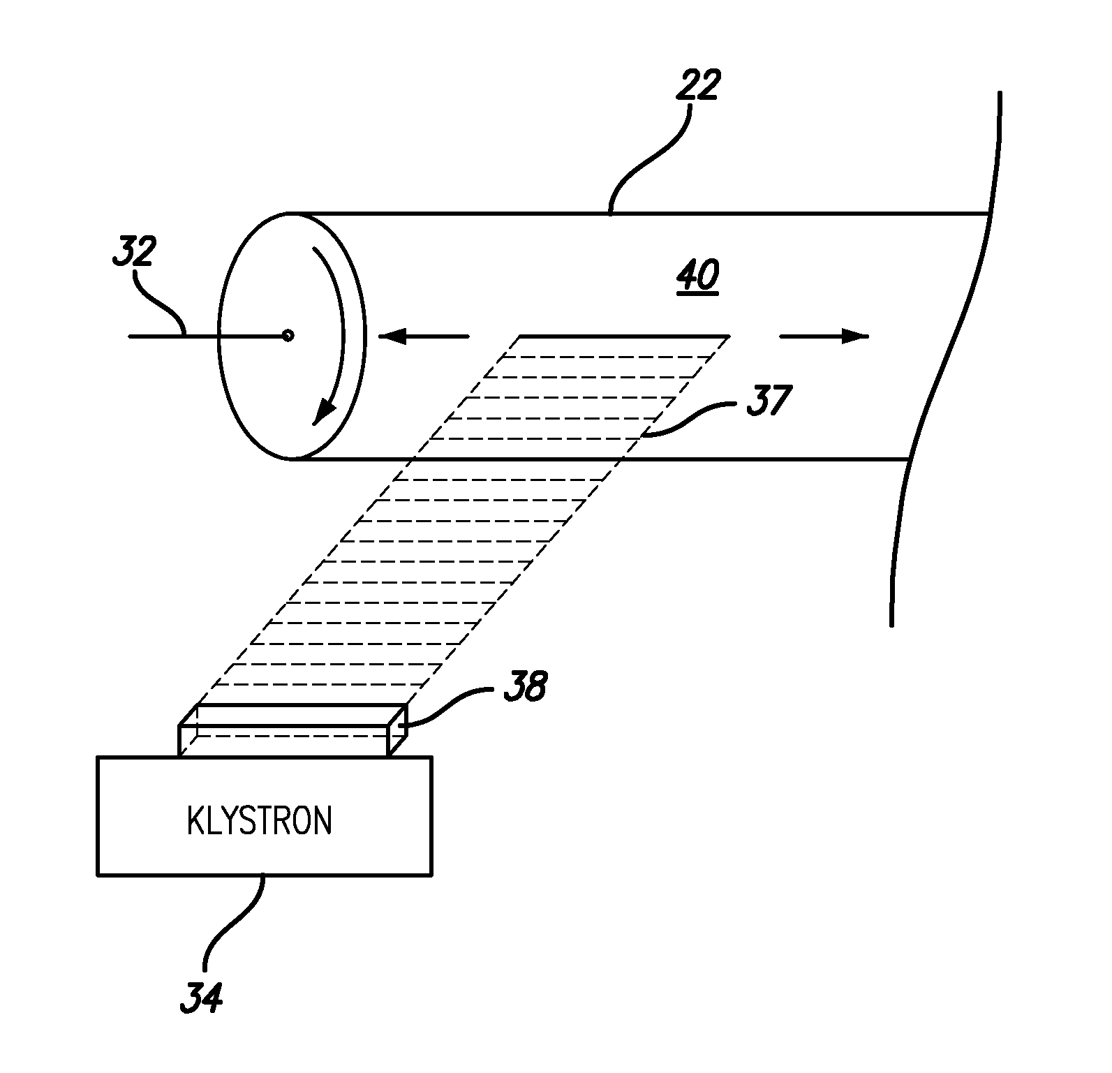
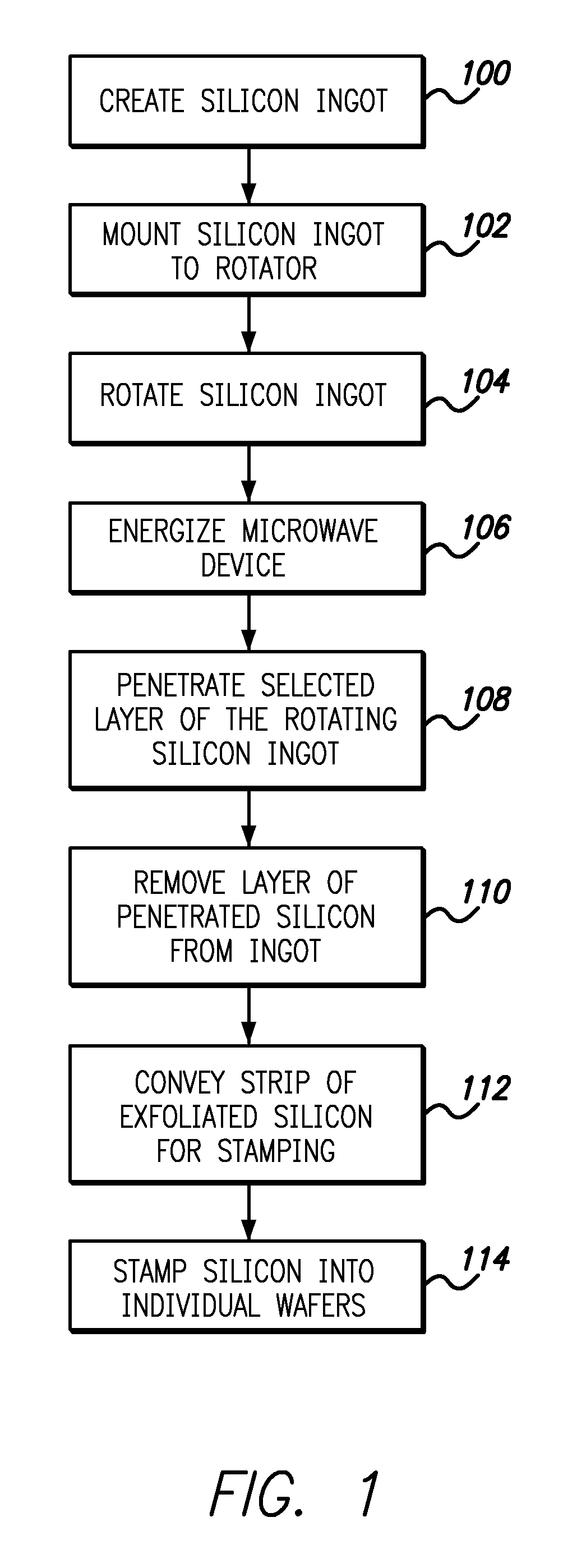
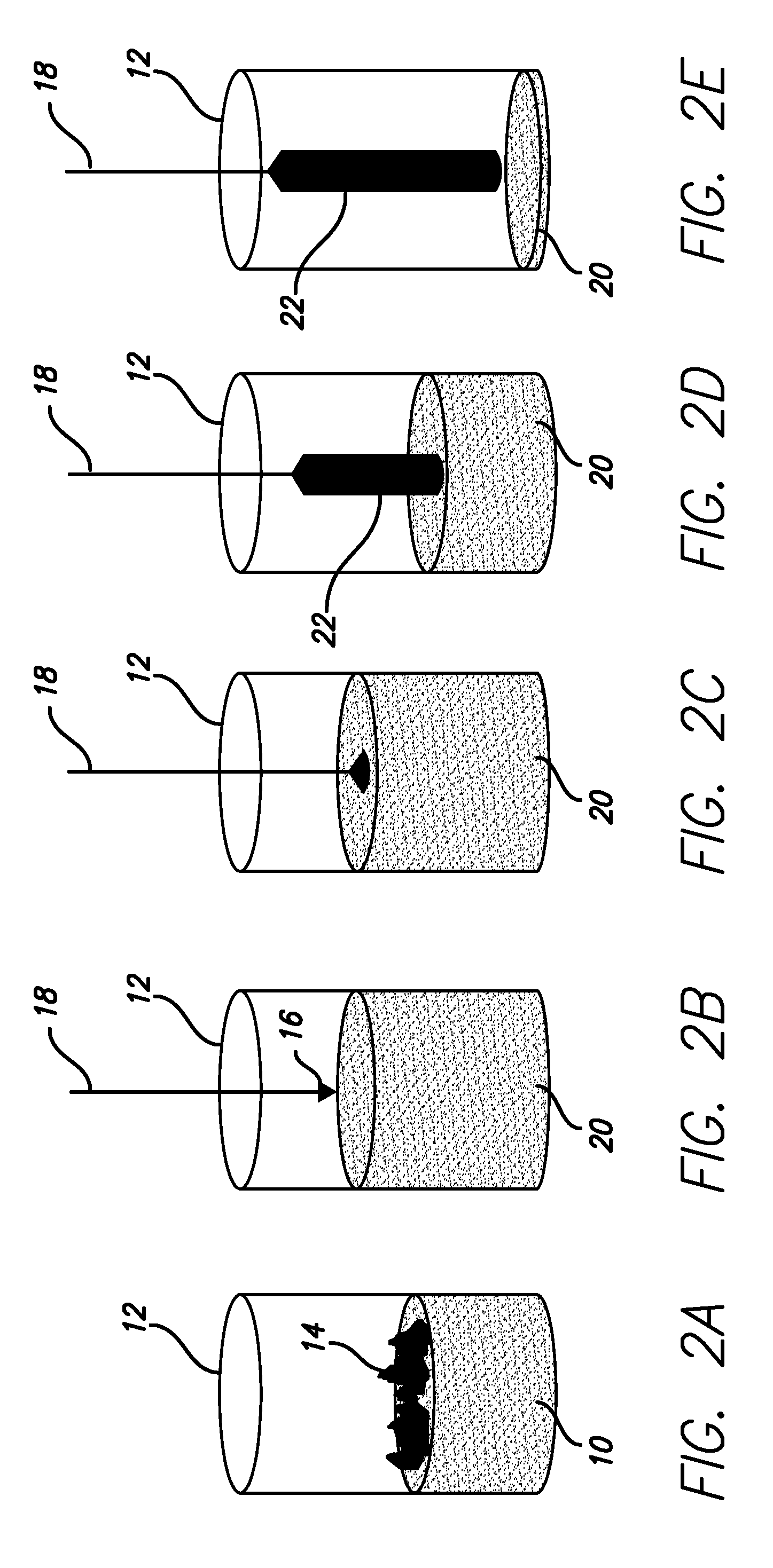
[0031]As shown in the drawings for purposes of illustration, the present invention for the improved processes for manufacturing wafers is shown generally with respect to the flowchart in FIG. 1 and the operation of the manufacturing process is shown in more detail in FIGS. 2-10. More specifically, the first step, as shown in FIG. 1, is to create an ingot 100. In a preferred embodiment, the ingot 100 is a monocyrstalline cylindrical silicon ingot. Although, the ingot 100 may be any material suitable for exfoliation, including polycrystalline silicon, and may have any cross-sectional shape, such as polygonal cross-sectional shape. The processes and apparatuses disclosed herein aim to, inter alia, reduce the waste associated with squaring off a cylindrical ingot used as a workpiece for creating square or rectangular silicon wafers for use with solar panels and the like. Furthermore, the processes and apparatuses disclosed herein are able to further reduce wasted wafer material by at le...


PUM

PropertyMeasurementUnit
widthaaaaaaaaaa
thicknessaaaaaaaaaa
diameteraaaaaaaaaa

Abstract

The process for manufacturing wafers includes the steps of mounting an ingot as a work piece in a manner that permits rotation about a longitudinal axis of rotation and rotating the ingot about its longitudinal axis of rotation to permit a microwave device that generates an energized beam to penetrate an outer surface layer thereof. Furthermore, the process includes exfoliating the outer surface layer with the energized beam, removing the exfoliated outer surface layer from the ingot as a continuous planar strip and cutting the continuous planar strip into a wafer.

Description

BACKGROUND OF THE INVENTION[0001]The present invention generally relates to processes and apparatuses for manufacturing wafers. More particularly, the invention relates to processes and apparatuses for exfoliating the external surface of an ingot to more efficiently produce solar grade photovoltaic wafers and the like therefrom.[0002]Conventionally, a wafer material such as monocrystalline silicon is processed into solar grade photovoltaic (“PV”) wafers by first creating a single crystalline cylindrical ingot of silicon. The ingot is created by melting high-purity semiconductor-grade wafer material in an inert chamber, such as one made of quartz. Dopant impurity atoms such as boron, phosphorus, arsenic, or antimony may be added to the molten wafer material in precise amounts (e.g., on the order of 1013 or 1016 atoms per cm3) to define the material as either a bulk n-type (negative) or p-type (positive) semiconductor, which gives the wafer material the desired electrical properties. ...

Claims


Application Information

Patent Timeline
Patent Type & Authority Patents(United States)
IPC IPC(8): C30B33/06B28D1/02B28D5/00C30B33/04C30B13/24C30B29/06
CPCC30B33/04B28D1/02B28D5/00C30B33/06C30B13/24C30B29/06
Inventor YAKUB, ANDREW X.
Owner RAYTON SOLAR
Features
  • R&D
  • Intellectual Property
  • Life Sciences
  • Materials
  • Tech Scout
  • Unparalleled Data Quality
  • Higher Quality Content
  • 60% Fewer Hallucinations
Learn More