Semiconductor laser apparatus and manufacturing method thereof

a laser and semiconductor technology, applied in semiconductor lasers, instruments, optical elements, etc., can solve the problems of high light propagation loss, inefficient heat dissipation, and accordingly degrading the life of the device, and achieve low propagation loss, high mechanical bond strength, and efficient heat dissipation

Active Publication Date: 2016-11-01
CLOUD LIGHT TECH LTD
View PDF3 Cites 1 Cited by
  • Summary
  • Abstract
  • Description
  • Claims
  • Application Information

AI Technical Summary

Benefits of technology

[0008]One objective of the present invention is to provide a semiconductor laser apparatus integrating an edge-emitting semiconductor laser (EEL) assembly with a silicon-on-insulator (SOI) assembly to obtain a single mode laser operation, which has low propagation loss, efficient heat dissipation and high mechanical bond strength.
[0009]Another objective of the present invention is to provide a method of manufacturing a semiconductor laser apparatus integrating an edge-emitting semiconductor laser assembly with a silicon-on-insulator assembly to obtain a single mode laser operation, which has low propagation loss, efficient heat dissipation and high mechanical bond strength.
[0036]In comparison with the prior art, when the laser light is emitted from the edge-emitting semiconductor laser assembly, the optical waveguide guides the laser light to confine within the core portion with lower transmission loss. Further, the light is confined in single mode due to the significant effective refractive index difference between the LD stack and the SOI stack that includes optical waveguide of silicon. Additionally, the multiple ribs of the waveguide are beneficial to reduce the junction temperature due to its high thermal conductivity, thereby increasing the life time for the optical device, and meanwhile, the corrugation ribs are also beneficial to enhance the mechanical bond strength between the bonding layer and the optical waveguide.

Problems solved by technology

However, the waveguide with a single silicon core (or rib) 104 or 130 will generate high light propagation loss, which requires high index difference between the LD stack and the waveguide of the SOI stack.
Also, due to lack of high thermal conductivity material just in between the full length of LD stack 102 and the single silicon core 104a or 134, the heat dissipation is inefficient, and the junction temperature (Tj) of the LD stack 102 increases and degrades the life time of device accordingly.

Method used


Image

  • Semiconductor laser apparatus and manufacturing method thereof
  • Semiconductor laser apparatus and manufacturing method thereof
  • Semiconductor laser apparatus and manufacturing method thereof

Examples


Embodiment Construction

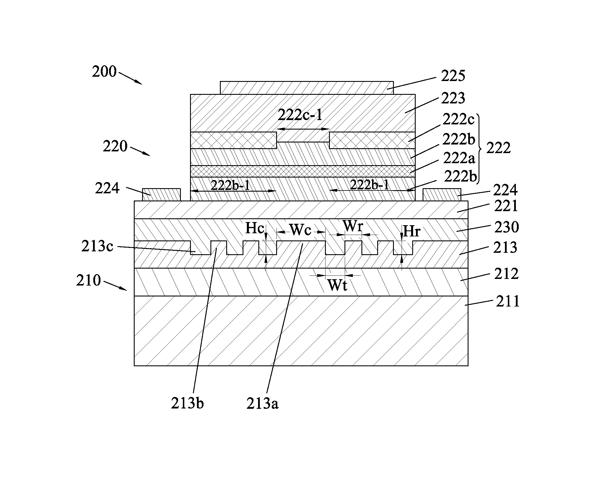
[0060]Various preferred embodiments of the invention will now be described with reference to the figures, wherein like reference numerals designate similar parts throughout the various views. As indicated above, the invention is directed to a semiconductor laser apparatus integrating an edge-emitting semiconductor laser (EEL) assembly (also called as LD stack, thereinafter) a silicon-on-insulator (SOI) assembly (also called as SOI stack, thereinafter) and a manufacturing method thereof to obtain an optical single mode operation, which has low loss propagation and high mechanical bond strength.

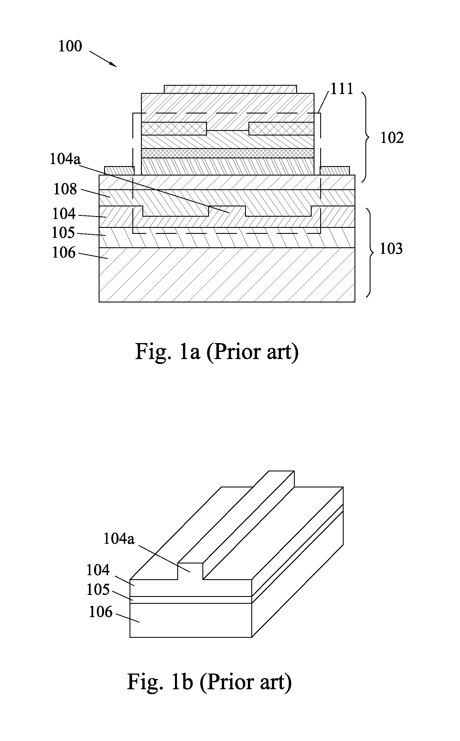
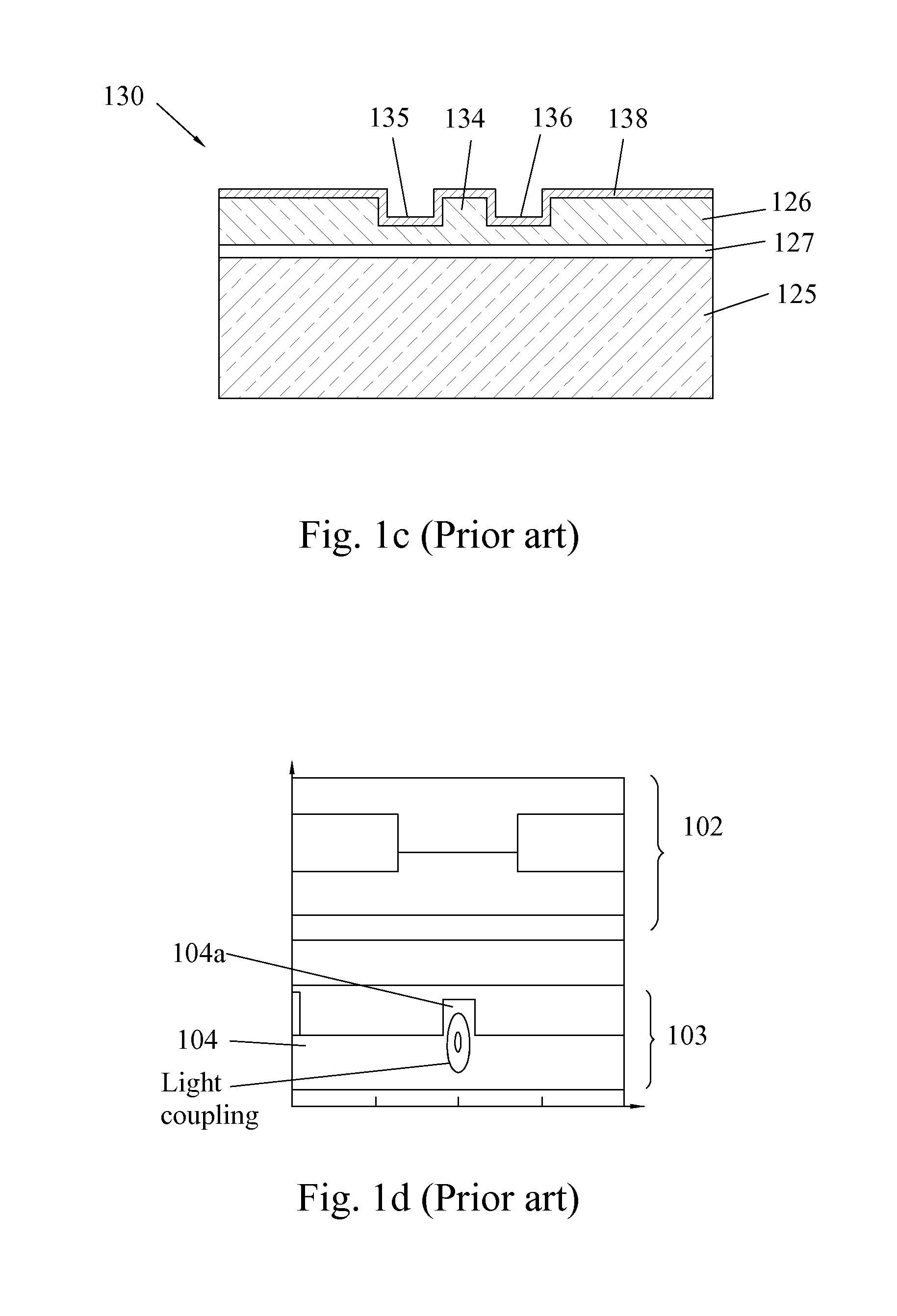
[0061]Referring to FIGS. 2a, 2b, 2c, the concept of evanescent coupling of light between the LD stack and SOI stack will be described generally, which is helpful to understand the present invention. In an EEL assembly (LD stack) 220, the light emits from edges of the laser through its cleaved facets as shown in FIG. 2a. These cleaved facets can also be coated by reflecting mirrors to extract li...


PUM


Abstract

A semiconductor laser apparatus includes a silicon-on-insulator assembly and an edge-emitting semiconductor laser assembly integrated on the silicon-on-insulator assembly. The silicon-on-insulator assembly includes an optical waveguide at the top which is bonded to the edge-emitting semiconductor laser assembly and configured to couple a laser light emitted from the edge-emitting semiconductor laser assembly, and the optical waveguide includes a core portion located in the middle of the optical waveguide; and at least one vertical rib configured on two sides of the core portion respectively, with a width narrower than that of the core portion. The apparatus obtains a single mode laser operation and has low propagation loss and high mechanical bond strength.

Description

FIELD OF THE INVENTION[0001]The present invention is related to a semiconductor laser apparatus, and more particularly to a semiconductor laser apparatus with an improved optical waveguide for evanescent coupling of light to form a single mode laser operation for high speed optical communication, and a manufacturing method thereof.BACKGROUND OF THE INVENTION[0002]In recent years, rapid increase of the Internet traffic has pushed the amount of data transmission sharply, and it has been demanded to increase the operation speed, as well as decrease the size and the cost for optical transmission and receiving equipment or optical components. Under the background described above, development has been conducted vigorously for silicon photonics that realize optical components by using silicon materials for making photonic integrated circuits (PIC) through CMOS processes instead of using optical components made on compound semiconductors such as GaAs and InP substrates directly.[0003]For pa...

Claims


Application Information

Patent Timeline
Patent Type & Authority Patents(United States)
IPC IPC(8): G02B6/42H01S5/12H01S5/02H01S5/022H01S5/125
CPCH01S5/1228G02B6/4206H01S5/021H01S5/02284H01S5/1203H01S5/02256H01S5/125G02B6/12002H01S5/02461H01S5/026H01S5/1032H01S5/3095G02B2006/12107G02B2006/12121G02B2006/12147H01S5/02251H01S5/02355
Inventor PADULLAPARTHI, BABU DAYAL
Owner CLOUD LIGHT TECH LTD
Why Eureka
Try Eureka