Wafer processing method

a processing method and wafer technology, applied in semiconductor/solid-state device testing/measurement, semiconductor device details, semiconductor devices, etc., can solve the problems of inability to accurately divide wafers, the cutting blade may be deviated or tilted, and the functional layer cannot be uniformly cut by the cutting blade. , to achieve the effect of accurately splitting the wafer

Active Publication Date: 2017-01-03
DISCO CORP
View PDF7 Cites 3 Cited by
  • Summary
  • Abstract
  • Description
  • Claims
  • Application Information

AI Technical Summary

Benefits of technology

[0006]It is therefore an object of the present invention to provide a wafer processing method which can accurately divide a wafer having a functional layer.
[0009]According to the wafer processing method of the present invention, the laser beam having a transmission wavelength to the substrate is applied to the wafer from the back side thereof to detect the height of the interface between the functional layer and the substrate in the area corresponding to each division line. The depth of cut by the cutting blade is next set according to the height detected above. The back side of the substrate is next cut by using the cutting blade according to the depth of cut set above to thereby form a cut groove having a depth not reaching the functional layer with a remaining part of the substrate left between the bottom of the cut groove and the functional layer along each division line, the remaining part having a uniform thickness. Thereafter, the remaining part and the functional layer are cut along each division line to thereby divide the wafer. Accordingly, the functional layer can be uniformly cut and the wafer can therefore be divided accurately.

Problems solved by technology

However, when the division of the functional layer in forming the laser processed grooves is insufficient, the cutting blade may be deviated or tilted.
As a result, the functional layer cannot be uniformly cut by the cutting blade and the wafer cannot be divided accurately.

Method used


Image

  • Wafer processing method
  • Wafer processing method
  • Wafer processing method

Examples


first preferred embodiment

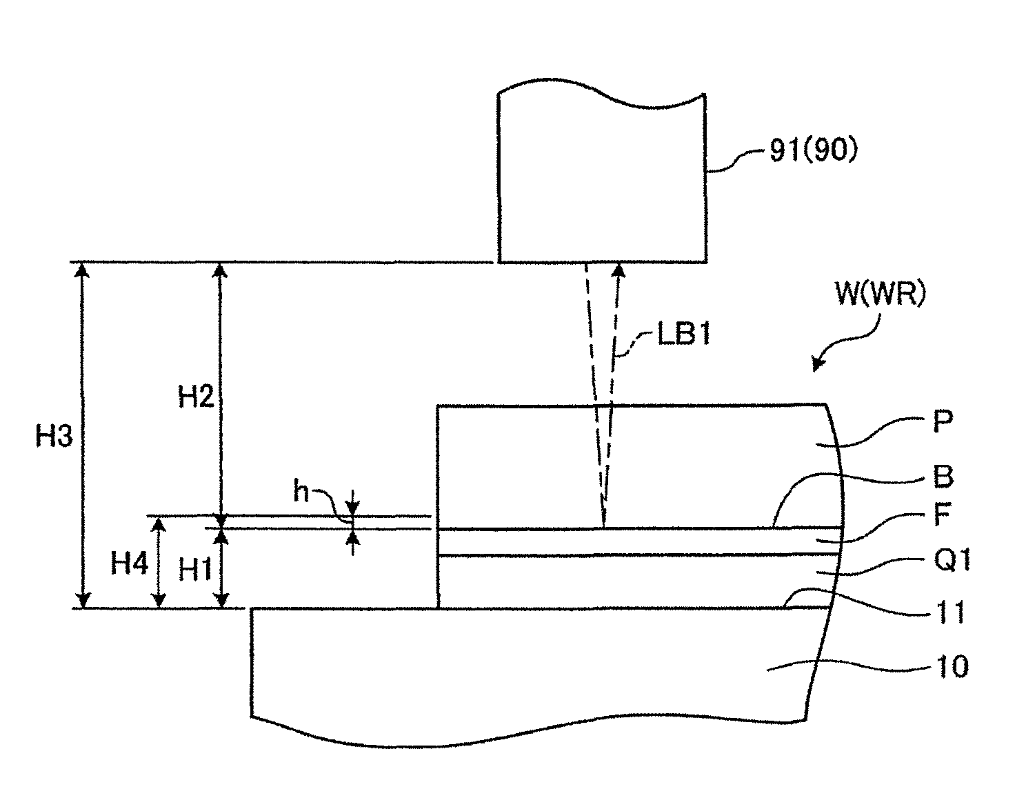
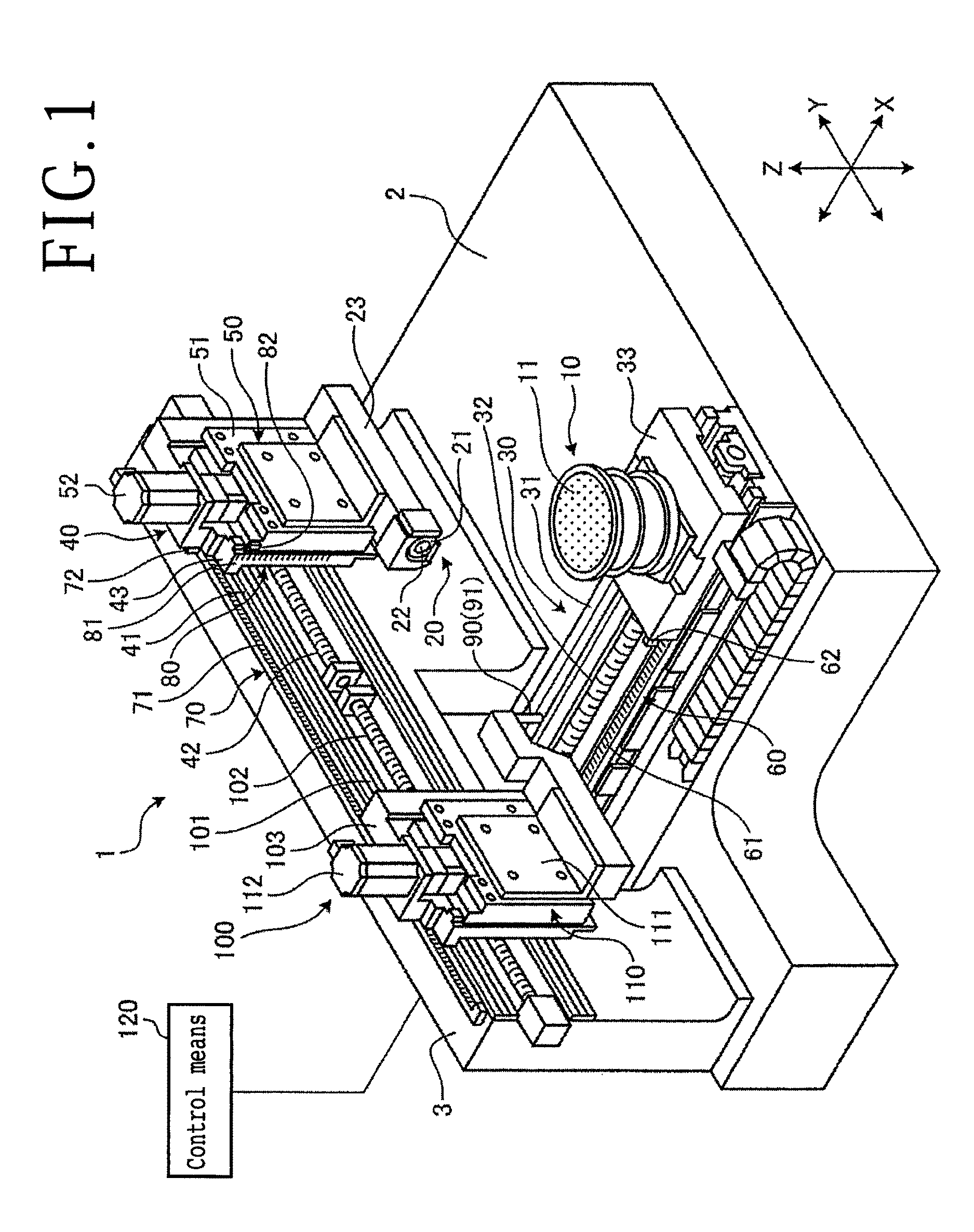
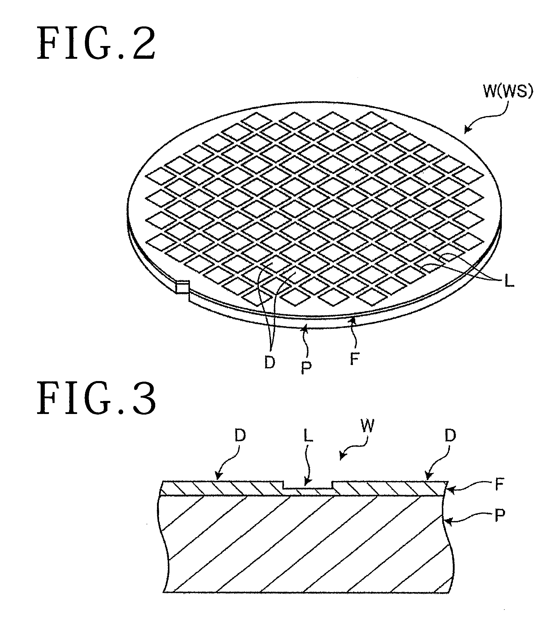
[0029]A first preferred embodiment of the wafer processing method according to the present invention will now be described. FIG. 1 is a perspective view showing the configuration of a cutting apparatus 1 for performing the first preferred embodiment. FIG. 2 is a perspective view showing the configuration of a wafer W to be processed by the cutting apparatus 1. FIG. 3 is a sectional view of the wafer W shown in FIG. 2. The cutting apparatus 1 is designed to cut the wafer W. As shown in FIG. 1, the cutting apparatus 1 includes a chuck table 10, cutting means 20, work feeding means (X moving means) 30, indexing means (first Y moving means) 40, cutter feeding means (first Z moving means) 50, X position detecting means 60, Y position detecting means 70, and Z position detecting means 80.

[0030]The wafer W includes various kinds of wafers such as a semiconductor wafer and an optical device wafer. The semiconductor wafer is composed of a substrate formed of silicon, gallium arsenide, etc. a...

second preferred embodiment

[0055]A second preferred embodiment of the wafer processing method according to the present invention will now be described. FIGS. 19 and 20 are sectional views showing a dividing step of dividing the wafer W by plasma etching according to the second preferred embodiment.

[0056]After forming the cut groove Pd on the back side WR of the wafer W along each division line L of the wafer W, a resist film R1 is formed on the back side WR of the wafer W in the area except each remaining part Pa as shown in FIG. 19. More specifically, the material of the resist film R1 is first applied to the whole of the back side WR of the wafer W, and next exposed to light through a predetermined mask pattern. Thereafter, the wafer W is immersed in a developer to thereby remove the resist film R1 from each remaining part Pa. Thus, the resist film R1 is formed on the back side WR of the wafer W in the area except each remaining part Pa. After forming the resist film R1 as mentioned above, the wafer W is su...

third preferred embodiment

[0057]A third preferred embodiment of the wafer processing method according to the present invention will now be described. FIGS. 21 and 22 are sectional views showing a dividing step of dividing the wafer W by using a cutting blade according to the third preferred embodiment.

[0058]After forming the cut groove Pd on the back side WR of the wafer W along each division line L of the wafer W, a cutting blade 21A having a thickness smaller than that of the cutting blade 21 is used to cut the remaining part Pa and the functional layer F along each division line from the back side WR of the wafer W, thereby forming a division groove Pf along each division line L as shown in FIGS. 21 and 22. In this manner, the remaining part Pa and the functional layer F along each division line L may be cut by using the cutting blade 21A rather than by using the laser processing apparatus 200 in the dividing step.


PUM


Abstract

Disclosed herein is a wafer processing method for dividing a wafer into a plurality of individual devices along a plurality of crossing division lines. The wafer is composed of a substrate and a functional layer formed on the front side of the substrate. The division lines are formed on the front side of the functional layer. A laser beam having a transmission wavelength to the substrate is applied to the wafer from the back side thereof to detect the height of an interface between the functional layer and the substrate in an area corresponding to each division line. The depth of cut by a cutting blade for cutting the substrate is next set according to the height detected above. The back side of the substrate is next cut by the cutting blade according to the depth of cut set above to thereby form a cut groove having a depth not reaching the functional layer with a remaining part of the substrate left between the bottom of the cut groove and the functional layer along each division line, the remaining part having a uniform thickness. Thereafter, the remaining part and the functional layer are cut along each division line to thereby divide the wafer.

Description

BACKGROUND OF THE INVENTION[0001]Field of the Invention[0002]The present invention relates to a wafer processing method.[0003]Description of the Related Art[0004]There has been put into practical use a manufacturing method for a semiconductor wafer having a plurality of semiconductor devices such as ICs and LSIs, wherein the semiconductor wafer is intended to improve the processing performance of the semiconductor devices. This semiconductor wafer is composed of a substrate and a functional layer formed on the front side of the substrate, wherein the functional layer is formed by stacking a plurality of low-permittivity insulator films (low-k films). Examples of each low-k film include an inorganic film of SiOF, BSG (SiOB), etc. and an organic film such as a polymer film of polyimide, parylene, etc. The semiconductor devices are formed from the functional layer of the wafer. The functional layer is brittle so that it is easily separated from the substrate in cutting the wafer by usi...

Claims


Application Information

Patent Timeline
Patent Type & Authority Patents(United States)
IPC IPC(8): H01L21/78H01L21/683H01L23/544H01L21/66
CPCH01L21/78H01L21/6836H01L22/26H01L23/544H01L2221/6834H01L2221/68327H01L2223/5446H01L21/6835H01L2221/68336H01L22/12H01L22/20H01L21/76H01L21/268
Inventor OGAWA, YUKINAGAOKA, KENSUKEOBATA, TSUBASABAN, YURI
Owner DISCO CORP
Why Eureka
Try Eureka