
Direct current control with low E-M emission

a technology of direct current supply and low e-m emission, which is applied in the direction of pulse technique, dc-dc conversion, power conversion system, etc., can solve the problems of increased electromagnetic emissions, substantial heat, damage to the circuit,

Active Publication Date: 2017-01-03
MELEXIS TECH NV
View PDF19 Cites 0 Cited by
  • Summary
  • Abstract
  • Description
  • Claims
  • Application Information

AI Technical Summary

Benefits of technology

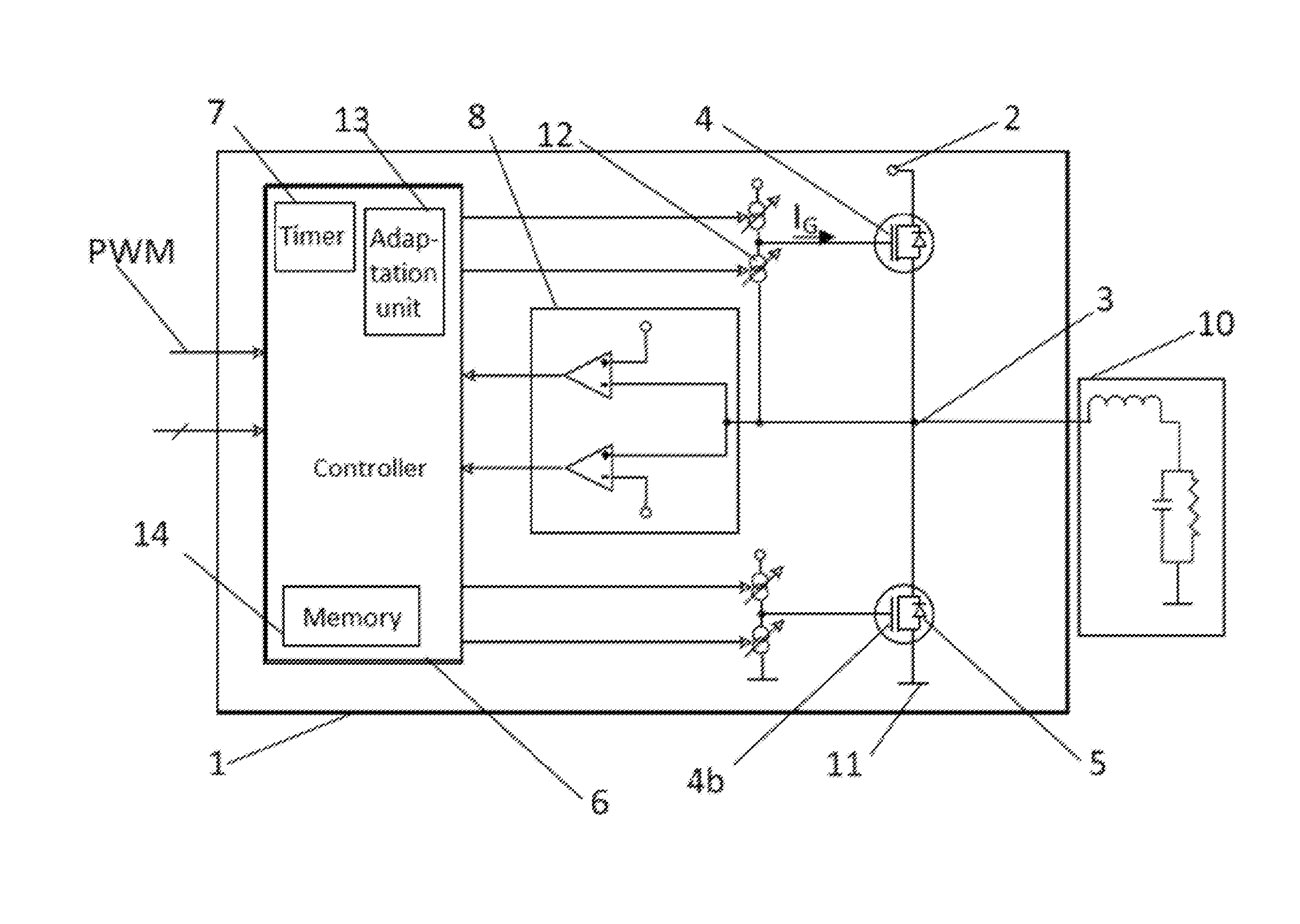
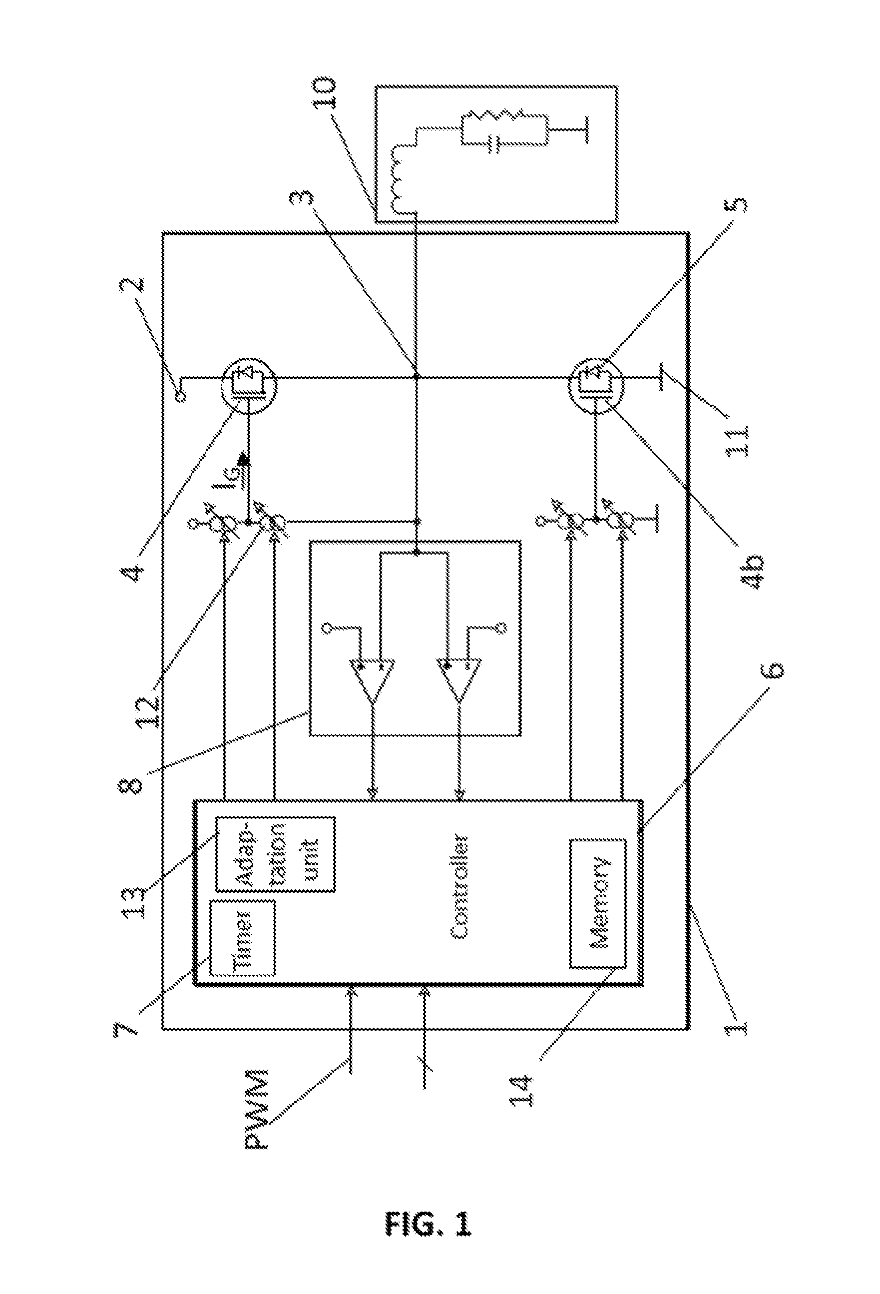
[0009]It is an object of embodiments of the present invention to provide efficient current modulation with low or limited electromagnetic emissions while controlling a DC current through an inductive load.
[0010]It is an advantage of embodiments according to the present invention that limited switching losses may be obtained while controlling a DC current through an inductive load.
[0011]It is an advantage of embodiments according to the present invention that high switching speeds may be obtained.

Problems solved by technology

The increased resistance of the transistor will therefore generate a substantial amount of heat, and may result in damage to the circuit if the gate voltage is reduced too fast with respect to the time needed for the flyback diode to divert the current flow.
This arrangement may reduce the undesirable effects of power dissipation in the semiconductor, but because the gate current is not reduced before the flyback diode starts to conduct, deep voltage transients at the deactivation of the switch might occur, which can lead to increased electromagnetic emissions.
Such emission may be avoided by reducing the initial discharge current to a lower level, which in turn leads to longer turn-off times and consequently increased overall power dissipation in the semiconductor switch.
Therefore the comparator delay is significantly increasing the power dissipation within the semiconductor switch because the increase of the charging current is delayed.
Although this method can reduce the discharge current to a low value when the free wheeling element starts to conduct, the method can only start to reduce the discharge current after the voltage on the flyback diode has started to drop, which may be too late to react for the current source to reduce its current, especially taking an additional delay of the measurement circuit into consideration.
This may lead to a rapid voltage change on the free wheeling element and may cause increased electromagnetic emissions.
In order to avoid such emissions, the initial discharge current must be reduced to a lower level, which in turn leads to longer turn-off times and consequently increased overall power dissipation in the semiconductor switch.

Method used


Image

  • Direct current control with low E-M emission
  • Direct current control with low E-M emission
  • Direct current control with low E-M emission

Examples


example 1

[0087]After a falling PWM input at T0 and if the assumed current direction through the load is positive (CDI=1)

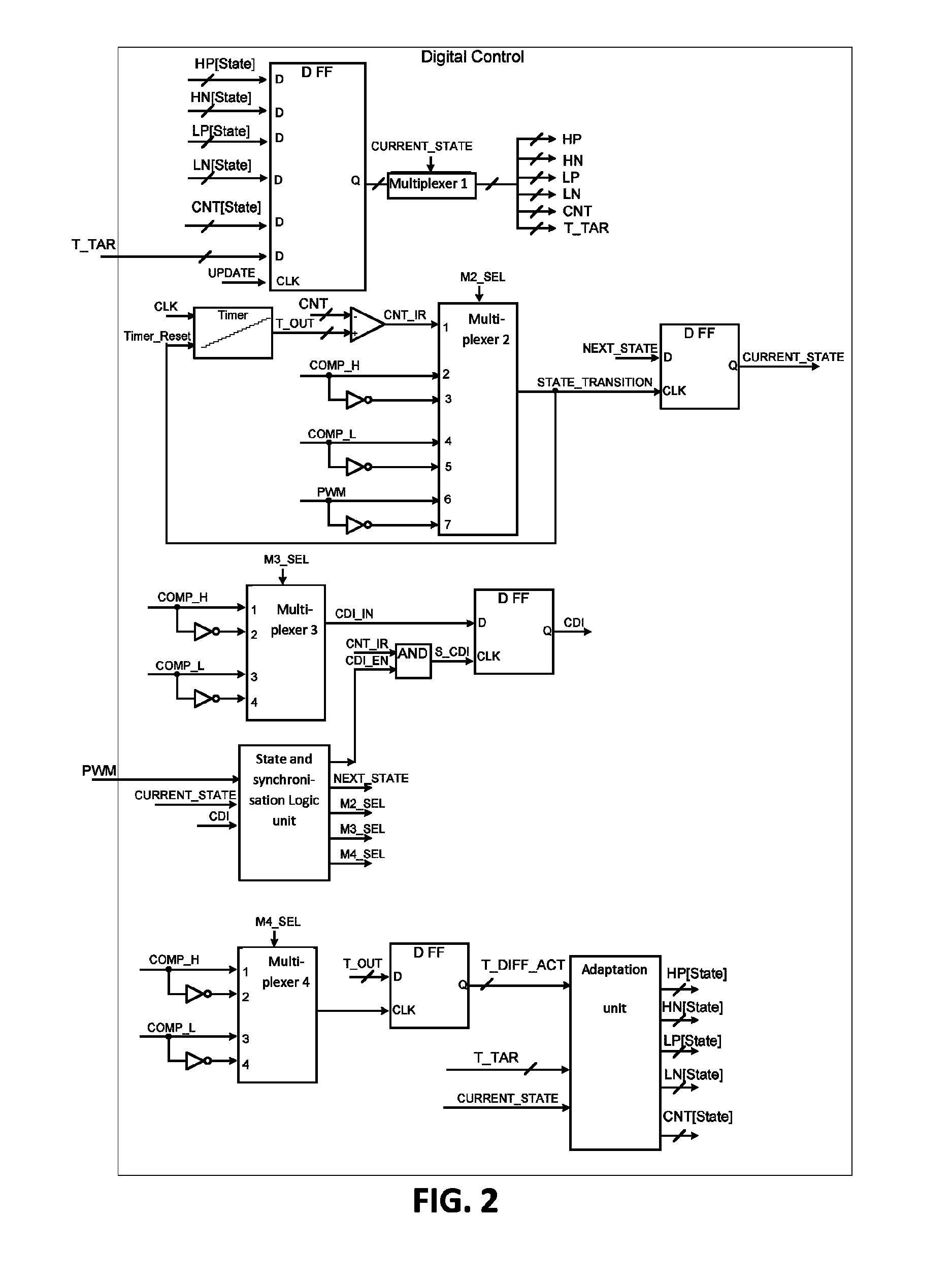
[0088]First the control gate of the HS FET is discharged with a discharge current strength HN[1] for a period of time CNT[1] and then it is reduced the discharge current to a lower value HN[2]. CNT[1] and HN[1] can either be predetermined or adapted parameters from a previous cycle in a way, that T1 occurs a desired target period of time T_TAR[2] before the terminal load voltage falls below a first reference voltage VERF_H. T_TAR[2] may be chosen to compensate any delay caused by the comparator and logic, in a way that the load voltage has not significantly changed before T1.

[0089]Taking a measure (TCF1) of the time difference between T1 and the instance in time when the terminal load voltage falls below a first reference voltage VERF_H during the current cycle and adapting parameter table entries CNT[1] and / or HN[1], so that T1 occurs a certain time prior to the terminal l...

example 2

[0103]After receiving a rising edge on the PWM input at time TR0 and if the assumed current direction thru the load is positive (CDI=1).

[0104]Discharging the gate of the LS FET with a discharge current strength LN[8] for a period of time CNT[8] and reducing the discharge current strength after the period of time at TR1. CNT[8] a predetermined or adapted parameter so that the discharge current is reduced before the current commutation from the LST to the LSD begins (change of diode voltage).

[0105]The duration CNT[8] and current strength LN[8] may be either predetermined or being adapted.

[0106]CNT[8] maybe calculated as

CNT[8]=Constant5*(CNT[1]*HN[1] / LN[8])

[0107]At TR1 discharging the gate of the LS FET with a discharge current strength LN[9] for a period of time CNT[9] and increasing the discharge current strength after the period of time at TR2. CNT[9] and LN[9] being either predetermined or being adapted parameter chosen in order that the current commutation from LST to LSD is compl...

example 3

[0125]After a falling PWM input at TF0 and if the assumed current direction thru the load is negative (CDI=0):

[0126]Discharging the gate of the HS FET with a discharge current strength HN[20] for a period of time CNT[20] and then to reduce the discharge current to a lower value HN[21].

[0127]CNT[20] a predetermined or adapted parameter so that the discharge current is reduced before the current commutation from the HST to the HSD begins (change of diode voltage).

[0128]CNT[20] maybe calculated as

CNT[20]=Constant20*(CNT[30]*LN[30] / HN[20])

[0129]At TF1 discharging the gate of the HS FET with a discharge current strength HN[21] for a period of time CNT[21] and increasing the discharge current strength after the period of time at TF2. CNT[21] and HN[21] being either predetermined or being adapted parameter chosen in order that the current commutation from LST to LSD is completed before TF2.

[0130]CNT[21] may be a function of CNT[30]:

CNT[21]=Constant21A−Constant21B*CNT[30]

[0131]CNT[22] and H...


PUM


Abstract

A switching control circuit includes driving a flow of direct current through an at least partially inductive load. The switching control circuit is adapted for adjusting a control current in order to activate and / or deactivate a flow of current to a load terminal. The system comprises a timer element for initiating at least one timed adjustment of the control current during activation or deactivation of the flow of current through a first semiconductor switch of the circuit so as to anticipate a state change of a component of the switching control circuit. The controller is adapted for determining a timing for the timed adjustment in a predictive manner. A method employs the various features of the switching control circuit.

Description

FIELD OF THE INVENTION[0001]The invention relates to the field of direct current supply control for inductive loads. More specifically it relates to a control circuit for turning on and off a direct current supply for an inductive load power circuit.BACKGROUND OF THE INVENTION[0002]Typically, a switching control circuit may be connected between a direct current power supply and a power load in series to obtain controlled activation and deactivation of the power load by an external trigger signal. When the impedance of the power load has a substantial inductive component, a free wheeling element, e.g. a flyback diode, may be placed in parallel to the power load to provide a path to conduct transient currents which are induced when altering the supplied voltage to the inductive load.[0003]A switching control circuit commonly comprises a semiconductor switch, for example a metal-oxide semiconductor field-effect transistor (MOSFET). In such MOSFET's, a voltage on the gate contact determ...

Claims


Application Information

Patent Timeline
Patent Type & Authority Patents(United States)
IPC IPC(8): H02M3/158H03K17/16H02M1/44
CPCH02M3/1588H02M1/44H03K17/166Y02B70/1466Y02B70/10
Inventor PAINTZ, CHRISTIANFREITAG, THOMASGRIMM, HEIKOREINHARDT, ENRICO
Owner MELEXIS TECH NV
Learn More