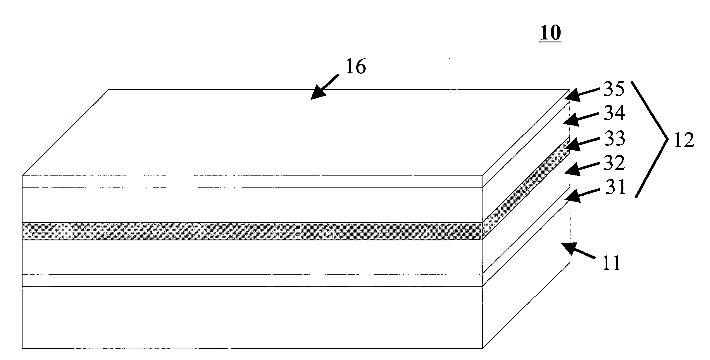
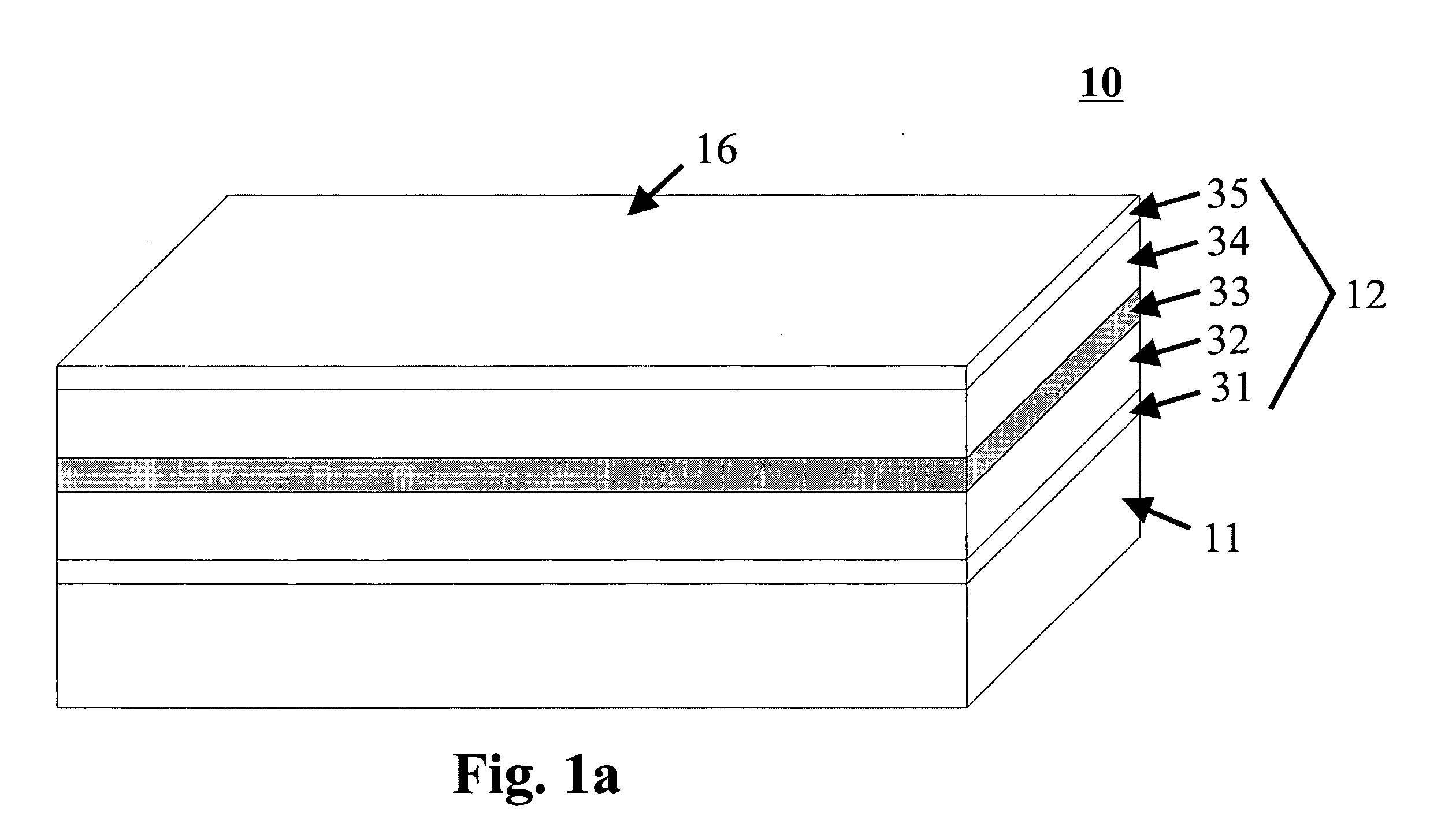
[0017] If a
metal is used to form the lattice structure, the advantageous effects described in the foregoing can be achieved to a particularly comprehensive extent. Irrespective of the material selected to construct the lattice structure, the lattice structure can also be formed by
material removal, not only by material application. In particular, the lattice structure can be formed as an overlying structure (e.g., a
metal lattice structure), as well as defined into the upper cladding layer by an etched structure and successive filling of the resulting grooves by other material (e.g., a
metal). Important in this context is the
close contact between lattice structure and upper
metallic electrode for efficient current injection to each of the cavity segments. If a metal is used to define the lattice structure, it is particularly advantageous to use the same metal also for the fabrication of the top
contact layer to each section. In particular, a metal layer sequence (e.g., Cr, Pt, Au
layers of various thickness) can also be used for this purpose. In order to improve the electrical injection, it proves advantageous for the sides of the waveguide ridge to be arranged substantially at right angles to the plane in which the lattice structure extends.
[0018] The typical semiconductor unipolar laser includes opposed front and back surfaces, referred to as front and back facets. These facets are typically obtained by cleaving. In order to control the light output and to direct it as desired, for example preferentially to the front side, it might become necessary to increase the back
facet reflectivity. Furthermore in order to realize other properties of the device, e.g., small threshold currents, it may be advisable to also increase the
reflectivity at the front surface. The
threshold current for laser onset is proportional to exp [2 (αi+αm) / Γgo], where Γ is the confinement factor, go is the material
gain, αi is the internal absorption and αm=1 / L*ln(1 / R) are the mirror losses. Therefore the
threshold current for any given laser length L can be significantly reduced if the
resonator reflectivity R is increased. By increasing the reflectivity, i.e., decreasing the mirror losses am, the length L of the device can be simultaneously reduced without a significant loss of performance as compared to lasers of the same lengths without additional reflectors. By using high
facet reflectivities, the
slope efficiency, i.e., the output power dependence on the drive current, can also be increased as compared to lasers with cleaved facets using highly reflective mirrors on one or both ends of the ridge.
[0019] This increase in reflectivity might, for example, be obtained by defining a Bragg reflector structure adjacent to the laser
facet(s). Typically a Bragg reflector structure is realized by applying different
dielectric materials of appropriate thickness to the facets. Since many
dielectric material have absorbing properties in the
wavelength range of interest, a particularly useful approach for a unipolar laser is the definition of a Bragg reflector using an air-semiconductor mirror structure. These reflectors are arranged perpendicular to the laser ridge at a certain distance from one or both ends. The width of the mirror plates as well as the width of the air gap depend on the emission wavelength of the device. The dimensions of the mirror plates can extend beyond the ridge widths dimensions to reduce
diffraction losses of the
laser light. By such a unipolar laser with Bragg mirrors at one or both end facets, particularly low current densities and high output powers can be achieved. This can be used to increase the upper temperature of laser operation with respect to devices with cleaved facets. The Bragg mirrors can be realized as mirror plates separated by gaps. Alternatively they can also be realised by a two dimensional periodic pattern involving for example air holes. In both cases the change of
refractive index can be used to modify the reflectivity compared to cleaved facets. Similar structures can also be used to control the
coupling between the unipolar laser segments. However, the Bragg mirrors are optional structures to modify the facet reflectivities which can be omitted if desired.
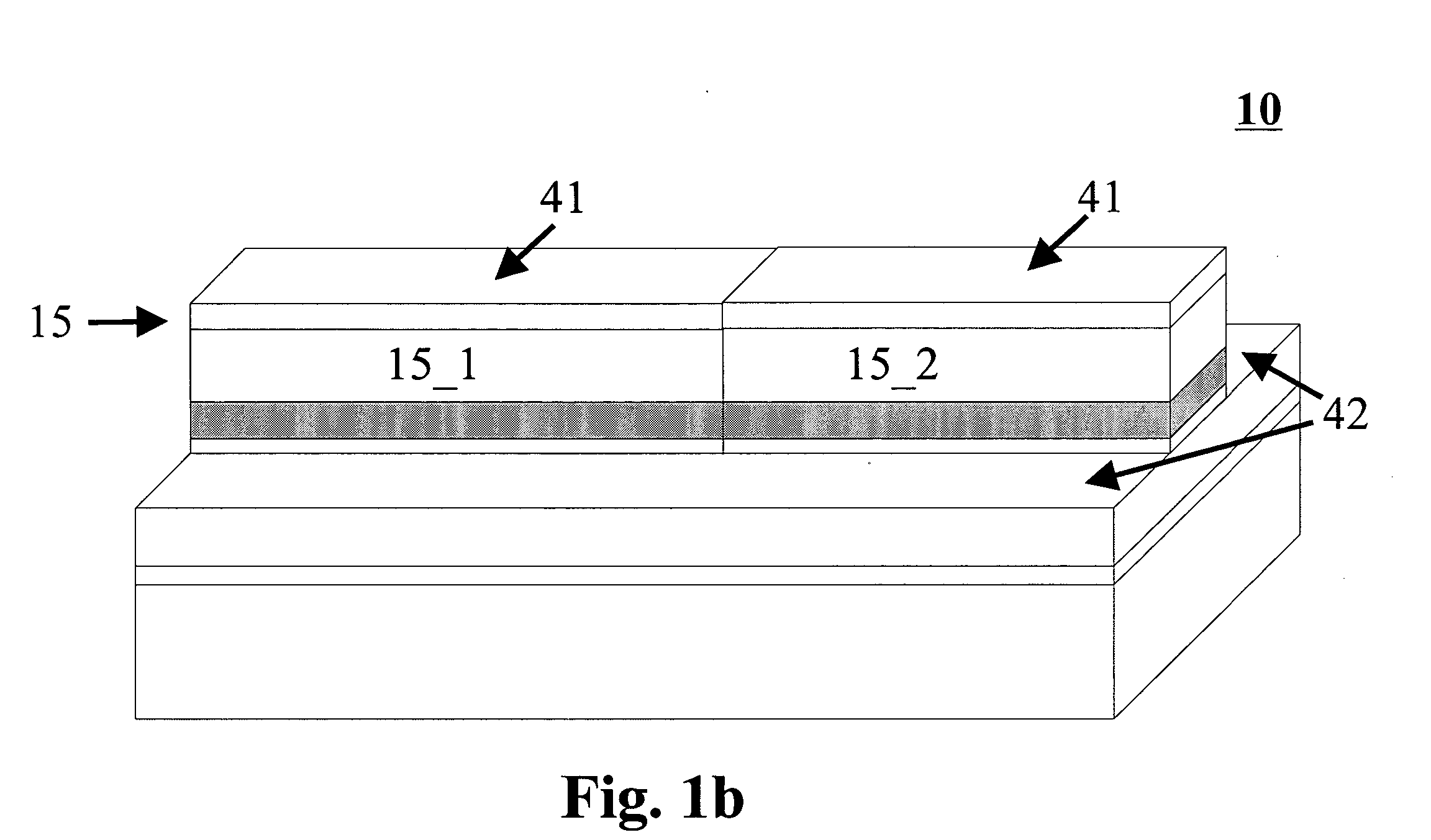
[0020] In a process according to the invention, on a base consisting of a semiconductor substrate, a complete unipolar semiconductor laser structure is produced in an epitaxial process with the subsequent formation of a waveguide ridge. This waveguide ridge is divided into a plurality of cavity sections by subjecting the semiconductor laser structure to a
material removal process and the subsequent application of a lattice structure to various cavity sections. Irrespective of the material selected to form the lattice structure, the lattice structure can also be produced by
material removal, not only by material application.
[0021] A processes according to the invention as briefly described in the foregoing thus facilitates the production of functional lasers in a first process phase, thereby facilitating the precise checking and determination of the electrical and optical properties, for example determination of the individual amplification spectrum of the epitaxial unipolar laser structure used for the
laser fabrication. Only thereafter in a second process phase, by the formation of cavity segments and lattice structures with defined parameters, are single-mode tuneable unipolar lasers obtained.
[0022] In those embodiments in which the lattice structure is produced by the application of a lattice, the use of a lithographic process, for example by optical or
electron beam
lithography with subsequent
etching of the lattice followed by a metallization, proves particularly advantageous.

