CMOS image sensor process and structure

a technology of image sensor and metal oxidesemiconductor, which is applied in the direction of semiconductor devices, diodes, electrical devices, etc., can solve the problem of ineffective reduction of dark current under the gate b>302/b>, and achieve the effect of improving the contrast of recorded images and reducing dark curren

Active Publication Date: 2008-05-29
UNITED MICROELECTRONICS CORP
View PDF10 Cites 21 Cited by
  • Summary
  • Abstract
  • Description
  • Claims
  • Application Information

AI Technical Summary

Benefits of technology

[0007]In view of the foregoing, this invention provides a CIS process that can reduce the dark current effectively and thereby improve the contrast of the recorded image.

Problems solved by technology

Thus, the dark current under the gate 302 cannot be decreased effectively.

Method used


Image

  • CMOS image sensor process and structure
  • CMOS image sensor process and structure
  • CMOS image sensor process and structure

Examples


first embodiment

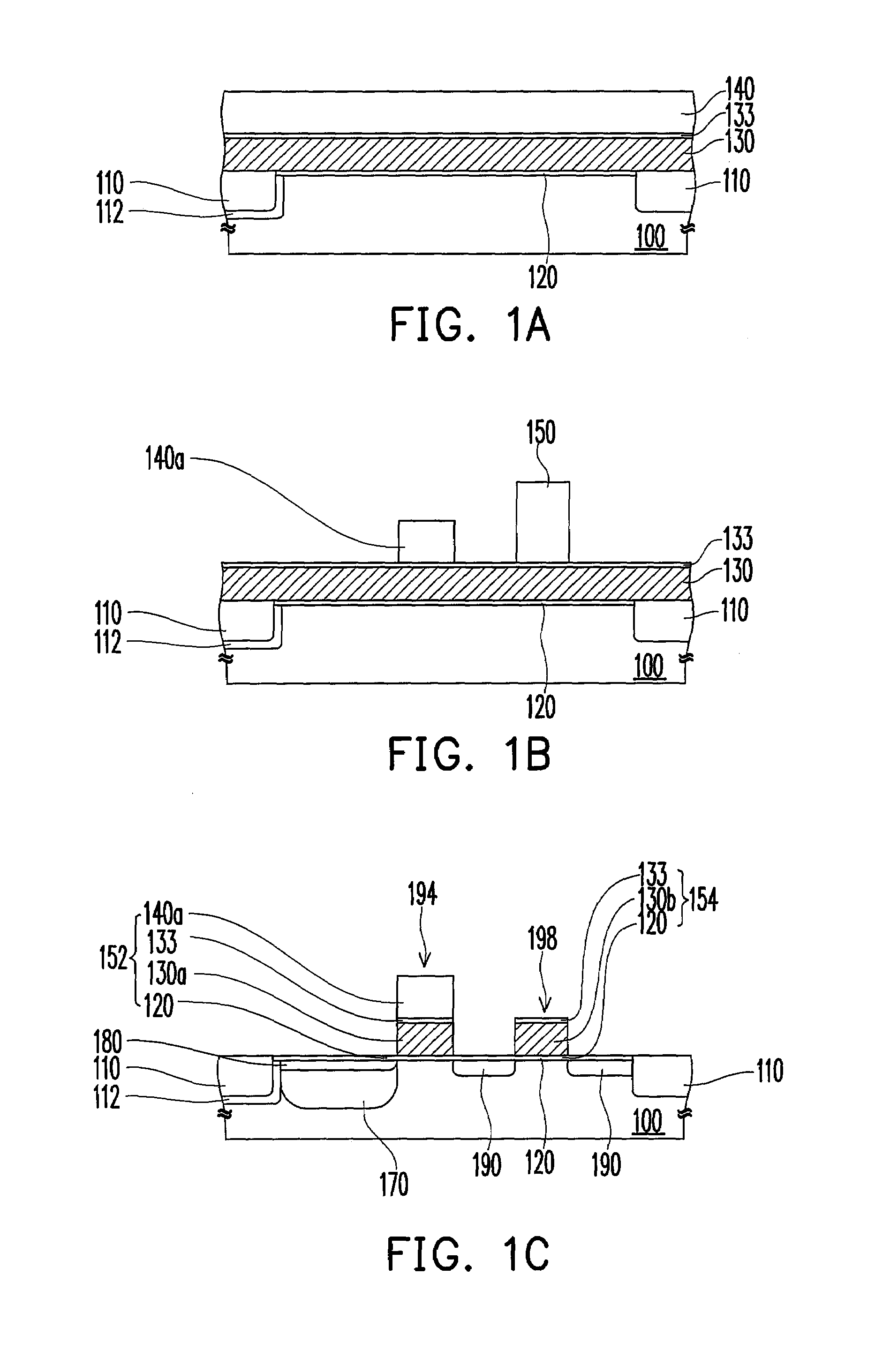
[0021]FIGS. 1A-1C illustrate, in a cross-sectional view, a CIS process according to the first embodiment of this invention, wherein the thickening layer is a hard mask layer.

[0022]Referring to FIG. 1A, a semiconductor substrate 100 like a p−-doped single-crystal Si-substrate is provided, possibly formed with an isolation structure 110 therein. The isolation structure 110 may be a shallow trench isolation (STI) structure or a field oxide layer formed with local Si-oxidation, and a portion thereof may be formed with a doped region 112 around as field isolation, wherein the conductivity type of the doped region 112 is the same as that of the substrate 100. Then, a gate dielectric layer 120, a gate material layer 130 and a hard mask layer 140 as a thickening layer are formed on the substrate 100 in sequence. The gate dielectric layer 120 may include silicon oxide formed through thermal oxidation, the gate material layer 130 may include poly-Si, and the hard mask layer 140 may include si...

second embodiment

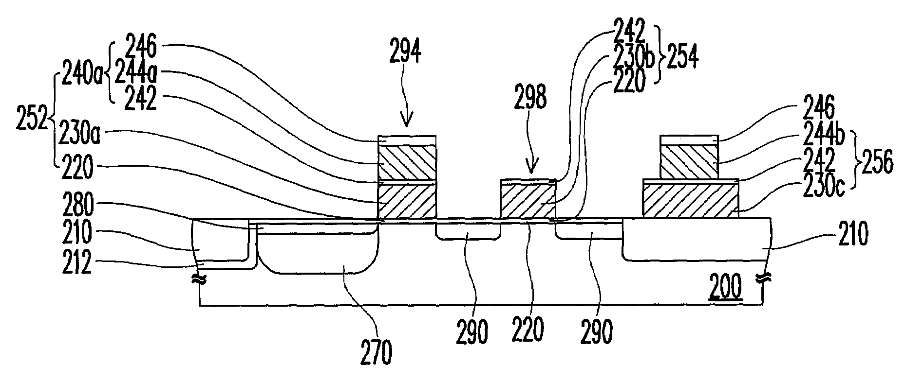
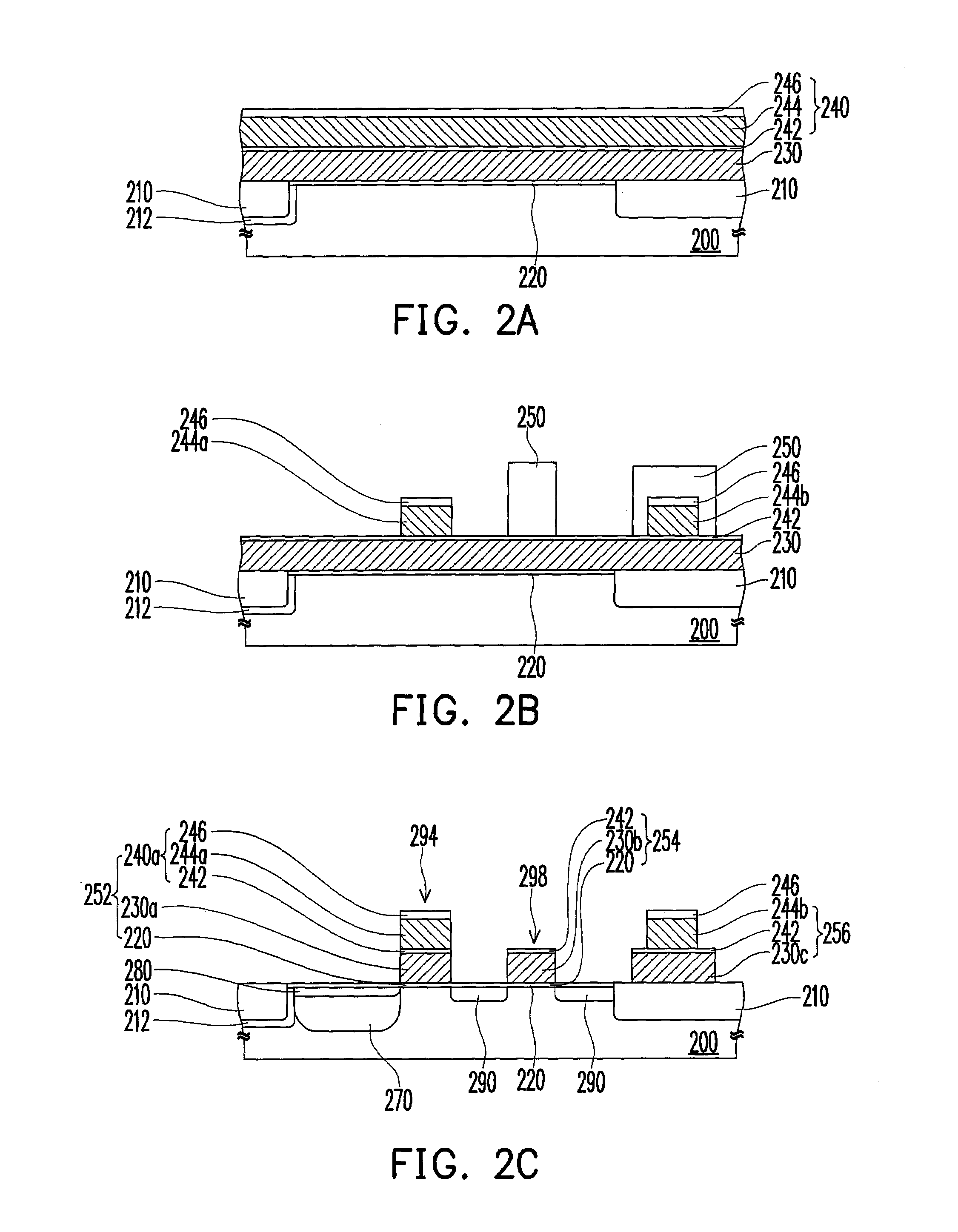
[0028]FIGS. 2A-2C illustrate, in a cross-sectional view, a CIS process according to the second embodiment of this invention, wherein the thickening layer is a composite layer including a dielectric layer, a conductive layer and a hard mask layer from bottom to top, and a capacitor is fabricated simultaneously with the gate structures.

[0029]Referring to FIG. 2A, a semiconductor substrate 200 formed with an isolation structure 210 therein is provided, wherein the isolation structure 210 may be the same as the above isolation structure 110, and a portion thereof may be formed with a doped region 212 around as field isolation like the above doped region 112. A gate dielectric layer 220, a gate material layer 230 and a thickening layer 240 are sequentially formed on the substrate 200, wherein the thickening layer 240 includes a dielectric layer 242, a conductive layer 244 and a hard mask layer 246 in the sequence of their formations. The materials of the gate dielectric layer 220 and the...


PUM


Abstract

A CMOS image sensor (CIS) process is described. A semiconductor substrate is provided, and then a gate dielectric layer, a gate material layer and a thickening layer are sequentially formed on the substrate, wherein the thickening layer includes at least a hard mask layer. The thickening layer is defined to form a transfer-gate pattern, and then the transfer-gate pattern is used as an etching mask to pattern the gate material layer and form a transfer gate. Ion implantation is then conducted to form a PN diode in the substrate with the transfer-gate pattern and the transfer gate as a mask.

Description

BACKGROUND OF THE INVENTION[0001]1. Field of Invention[0002]The present invention relates to fabrication and structures of a semiconductor device, and more particularly to a complementary metal-oxide-semiconductor (CMOS) image sensor (CIS) process and a CIS structure.[0003]2. Description of Related Art[0004]The CMOS image sensor is utilized more and more widely in image recording as compared with the charge-coupled device (CCD), for its fabricating process can be easily integrated with a conventional CMOS process lowering the manufacturing cost.[0005]A typical CMOS image sensor includes a PN diode for absorbing incident light to produce charges, and a transfer transistor for transferring the charges. Referring to FIG. 3, in a conventional CIS process, the gate 302 of the transfer transistor is formed on a substrate 300, and a photoresist pattern 304 is formed exposing an area of the substrate 300 predetermined for forming the diode, wherein a portion of the gate 302 is usually expos...

Claims


Application Information

Patent Timeline
Patent Type & Authority Applications(United States)
IPC IPC(8): H01L31/0224H01L21/8238
CPCH01L27/14689H01L27/14643
Inventor KAO, CHING-HUNG
Owner UNITED MICROELECTRONICS CORP
Why Eureka
Try Eureka