
Stacked rows pseudo-randomly spaced two-dimensional phased array assembly

Active Publication Date: 2017-01-31
HRL LAB
View PDF16 Cites 38 Cited by
  • Summary
  • Abstract
  • Description
  • Claims
  • Application Information

AI Technical Summary

Benefits of technology

The present patent describes a phased array optical beam former module that can independently and simultaneously point and steer multiple beams of light in three wavelength bands through a single, compact output aperture. The module is compact, mechanically rigid, and can be easily integrated with a CMOS electronic controller circuit. Compared to other non-mechanical beam steering alternatives, the module is more stable, compatible with a variety of laser sources and laser wavelengths over multiple bands, and can simultaneously form and steer multiple beams over a larger field of regard with faster response times. The output aperture contains a bi-dimensional array of optical microlenses, with each microlens functioning to increase the divergence of the shorter-wavelength light emitted from its emitter aperture and also to prevent optical crosstalk between adjacent array elements. The lens coupled to the single aperture is adapted to increase the divergence of light of the first wavelength emitted from the aperture.

Problems solved by technology

However, a main limitation of the liquid crystal based optical phased array is its slow steering speed (10's of millisecond range) which is due to the slow response time of the liquid crystal-based phase shifting elements.
Another disadvantage of liquid crystals is that they operate over a limited temperature range.
Consequently, for practical purposes, the operating temperature of the liquid crystal based optical phased array should be externally controlled, which further adds to its complexity.
Another problem with the liquid crystal based optical phased array is the presence of grating lobes in the steered beam, which not only severely reduces the optical efficiency of the phased array but also requires complex signal detection circuitry when used in a receiver.
Reducing the strip width below 5 μm results in a significant field-fringing effect and correspondingly reduces the electro-optic efficiency of the device, since the thickness of the liquid crystal cell is about 4 μm.
An important limitation of using optical fibers is that the minimum spacing between adjacent emitter is very large and thus the average side lobe power is fairly high.
For at least the above reasons, achieving a two-dimensional optical phased array using one or more mono-dimensional arrays of phase shifters and capable of steering an output optical beam over a large field of regard (e.g., +45-60°) along two orthogonal axes has been difficult.
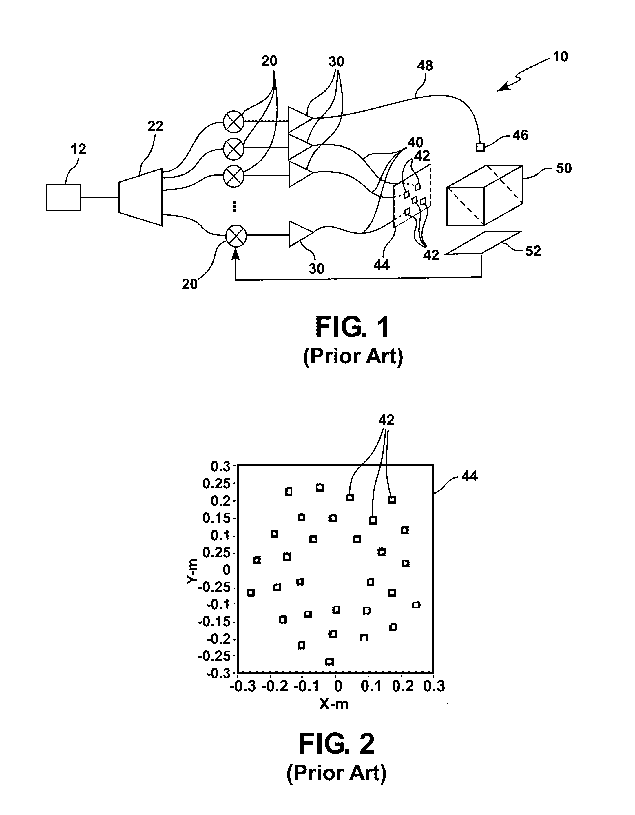
Another deficiency of known phased arrays such as phased array 10 is that the phase of the light output from the fibers 40, 48 can fluctuate as a result of mechanical vibrations or changes in ambient temperature, thus detrimentally affecting the operation of optical phased array 10.
However, it is difficult to fabricate an optical phased array having a λ / 2 element spacing, especially for phased arrays that operate overall the SWIR, MWIR1, MWIR2 or LWIR wavelength bands.

Method used


Image

  • Stacked rows pseudo-randomly spaced two-dimensional phased array assembly
  • Stacked rows pseudo-randomly spaced two-dimensional phased array assembly
  • Stacked rows pseudo-randomly spaced two-dimensional phased array assembly

Examples


Embodiment Construction

[0114]In the following description, numerous specific details are set forth to clearly describe various specific embodiments disclosed herein. One skilled in the art, however, will understand that the presently claimed invention may be practiced without all of the specific details discussed below. In other instances, well known features have not been described so as not to obscure the invention.

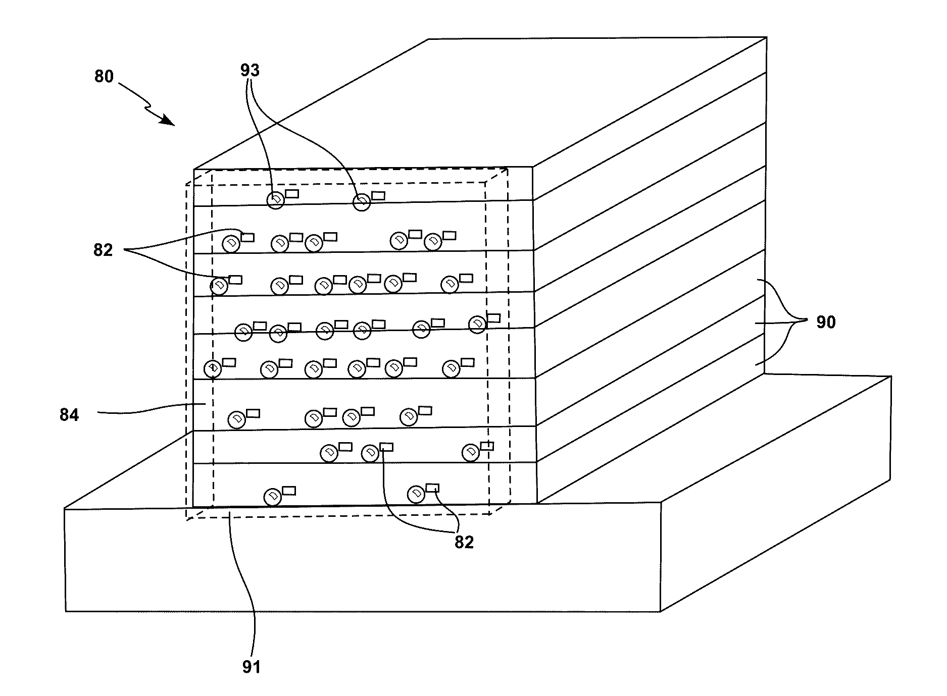
[0115]FIG. 4A shows a front view of a phased array 80 according to an embodiment of the present disclosure, comprising a predetermined number of optical emitter / receiver elements 82 arranged along an array 84 comprising stacked rows, wherein the optical emitter / receiver elements 82 in each row of the array are distributed according to a pseudo-random pattern; and the height of each row varies according to a pseudo-random pattern. According to an embodiment of the present disclosure, the height of each row varies within a first predetermined range along a first pseudo random pattern. Similarly...


PUM


Abstract

A phased array that comprises a predetermined number of emitter / receiver elements; said emitter / receiver elements being arranged on a array formed of stacked rows, wherein the emitter / receiver elements in each row of the array are distributed according to a pseudo-random pattern; and the heights of the rows vary according to a pseudo-random pattern.

Description

CROSS REFERENCE TO RELATED APPLICATIONS[0001]The present disclosure claims priority of U.S. provisional application No. 61 / 829,194, filed on May 30, 2013 and entitled “MULTI-WAVELENGTH OPTICAL BEAM FORMER”, which is hereby incorporated by reference.REFERENCE TO A CONTRACT[0002]This disclosure relates to work performed under Government contract No. N00014-13-C-0036; entitled “MULTI-BAND OPTICAL PHASED ARRAY BEAM FORMER”.INCORPORATION BY REFERENCE[0003]The present disclosure relates to co-pending U.S. patent Ser. No. 14 / 290,986, filed on May 29, 2014 and entitled: “MULTI-SLICE TWO-DIMENSIONAL BEAM FORMER ASSEMBLY”, which is hereby incorporated by reference.[0004]The present disclosure relates to co-pending U.S. patent Ser. No. 14 / 290,979, filed on May 29, 2014 and entitled: “MULTI-WAVELENGTH BAND OPTICAL PHASE AND AMPLITUDE CONTROLLER”, which is hereby incorporated by reference.TECHNICAL FIELD[0005]The present disclosure relates to phased arrays, and in particular to a two-dimensional...

Claims


Application Information

Patent Timeline
IPC IPC(8): G02F1/25G02B3/06G01S7/495G02F1/025G01S7/481G02B3/00H01L25/16G02F1/015
CPCG02F1/025G01S7/4813G01S7/495G02B3/0006H01L25/167G02F2001/0151G02B3/0056G01S7/4817G02F1/2955G02F1/0147G02F1/0151G02B6/10G01S7/4815G01S13/4463H01L21/76879H01L23/481H01L23/49827H01L23/5226H01L33/62H01L33/64
Inventor YAP, DANIELGEARY, KEVINWHITE, CARSON R.
Owner HRL LAB
Learn More