Semiconductor device and method for reduced bias temperature instability (BTI) in silicon carbide devices

a silicon carbide and semiconductor technology, applied in semiconductor devices, semiconductor/solid-state device details, electrical apparatus, etc., to achieve the effect of reducing the threshold voltage shift of the mosfet device during operation and reducing the pressure environmen

Active Publication Date: 2017-02-21
GENERAL ELECTRIC CO
View PDF63 Cites 2 Cited by
  • Summary
  • Abstract
  • Description
  • Claims
  • Application Information

AI Technical Summary

Benefits of technology

[0005]In another embodiment, a metal-oxide field-effect transistor (MOSFET) device includes an enclosure disposed about the MOSFET device. The enclosure is configured to surround the MOSFET device in a reduced pressure environment relative to an environment outside of the enclosure. Further, the reduced pressure environment reduces a threshold voltage shift of the MOSFET device during operation.
[0006]In another embodiment, a method includes providing a silicon carbide (SiC) electrical device and sealing the SiC electrical device in a package under an atmosphere having a pressure less than approximately 10 torr. The atmosphere inhibits negative bias temperature instability (NBTI) when operating the SiC electrical device at elevated temperatures, elevated biases, or both, for an extended period of time.

Problems solved by technology

Further, the particular atmosphere limits a shift in a threshold voltage of the SiC semiconductor device to less than 1 V during operation.
Further, the reduced pressure environment reduces a threshold voltage shift of the MOSFET device during operation.

Method used


Image

  • Semiconductor device and method for reduced bias temperature instability (BTI) in silicon carbide devices
  • Semiconductor device and method for reduced bias temperature instability (BTI) in silicon carbide devices
  • Semiconductor device and method for reduced bias temperature instability (BTI) in silicon carbide devices

Examples


Embodiment Construction

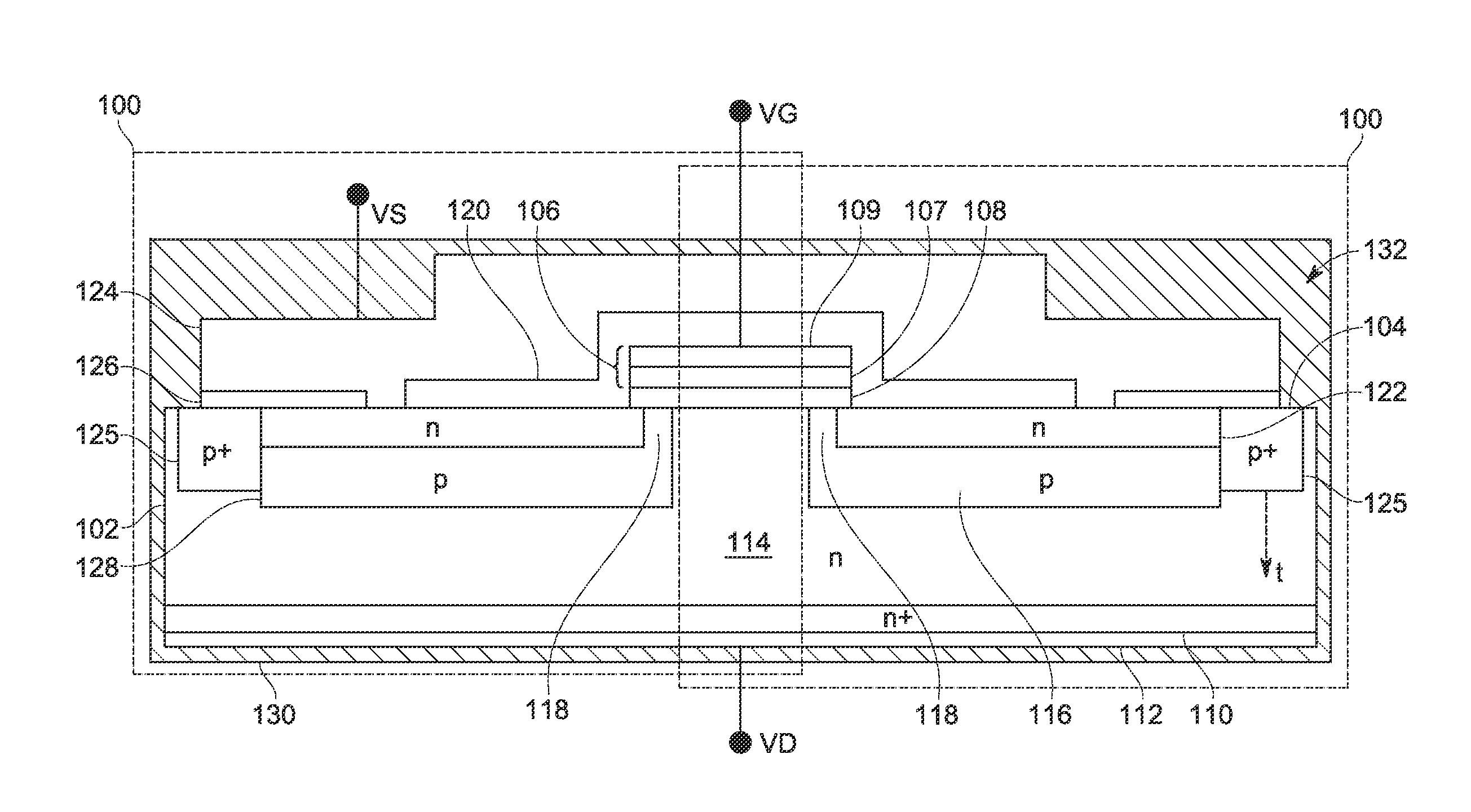
[0015]One or more specific embodiments will be described below. In an effort to provide a concise description of these embodiments, all features of an actual implementation may not be described in the specification. It should be appreciated that in the development of any such actual implementation, as in any engineering or design project, numerous implementation-specific decisions must be made to achieve the developers' specific goals, such as compliance with system-related and business-related constraints, which may vary from one implementation to another. Moreover, it should be appreciated that such a development effort might be complex and time consuming, but would nevertheless be a routine undertaking of design, fabrication, and manufacture for those of ordinary skill having the benefit of this disclosure.

[0016]When introducing elements of various embodiments of the present invention, the articles “a,”“an,”“the,” and “said” are intended to mean that there are one or more of the ...


PUM


Abstract

A system includes a silicon carbide (SiC) semiconductor device and a hermetically sealed packaging enclosing the SiC semiconductor device. The hermetically sealed packaging is configured to maintain a particular atmosphere near the SiC semiconductor device. Further, the particular atmosphere limits a shift in a threshold voltage of the SiC semiconductor device to less than 1 V during operation.

Description

BACKGROUND[0001]The subject matter disclosed herein relates to semiconductor devices and, more specifically, to silicon carbide semiconductor devices.[0002]For a semiconductor device, such as a silicon (Si) or silicon carbide (SiC) transistor, bias temperature instability (BTI) may cause substantial variability in device performance. For example, negative bias temperature instability (NBTI) in particular may result in a significant change or drift in the threshold voltage of a SiC device when operated under particular conditions, such as negative bias and / or elevated temperatures, over an extended period of time. The NBTI in SiC devices is thought to be a result of interfacial charge trapping (e.g., oxide charges), which may, for example, be induced by operating the device at an elevated temperature, and under a particular bias condition, for extended time periods. For example, a SiC metal-oxide-semiconductor field effect transistor (MOSFET) may experience a threshold voltage shift ...

Claims


Application Information

Patent Timeline
Patent Type & Authority Patents(United States)
IPC IPC(8): H01L21/56H01L23/04H01L21/50H01L29/78H01L29/16
CPCH01L23/04H01L21/50H01L29/1608H01L29/7802H01L2924/0002H01L2924/00
Inventor MICHAEL, JOSEPH DARRYLARTHUR, STEPHEN DALEY
Owner GENERAL ELECTRIC CO
Why Eureka
Try Eureka