Carbon nanotube field-effect transistor with sidewall-protected metal contacts

a technology of carbon nanotube transistors and metal contacts, which is applied in the direction of semiconductor devices, basic electric elements, electrical equipment, etc., can solve the problems of low yield and unstable nfets in device fabrication, severe degradation, and dramatic deformation of contact properties, so as to and prevent degradation of metal contacts

Inactive Publication Date: 2017-02-21
IBM CORP
View PDF11 Cites 11 Cited by
  • Summary
  • Abstract
  • Description
  • Claims
  • Application Information

AI Technical Summary

Benefits of technology

[0006]A field effect transistor includes a substrate and a gate dielectric formed on the substrate. A channel material is formed on the dielectric layer. The channel material includes carbon nanotubes. A patterned resist layer has openings formed therein. Metal contacts are formed on the channel material in the openings in the patterned resist layer and over portions of the patterned resist layer to protect sidewalls of the metal contacts to prevent degradation of the metal contacts.
[0007]A field effect transistor includes a semiconductor substrate configured to form a gate electrode, a gate dielectric formed on the substrate and carbon nanotubes formed on the dielectric layer to form a channel. A patterned resist layer has openings formed therein, and n-type metal contacts are formed on the carbon nanotubes in the openings in the patterned resist layer. The metal contacts include extension regions whi

Problems solved by technology

While CNT p-type metal contacts (typically Pd) have been extensively studied and proven to be air-stable and robust, n-type metal contacts (typically Sc and Er) are usually prone to react with oxygen and hence suffer from seve

Method used


Image

  • Carbon nanotube field-effect transistor with sidewall-protected metal contacts
  • Carbon nanotube field-effect transistor with sidewall-protected metal contacts
  • Carbon nanotube field-effect transistor with sidewall-protected metal contacts

Examples


Embodiment Construction

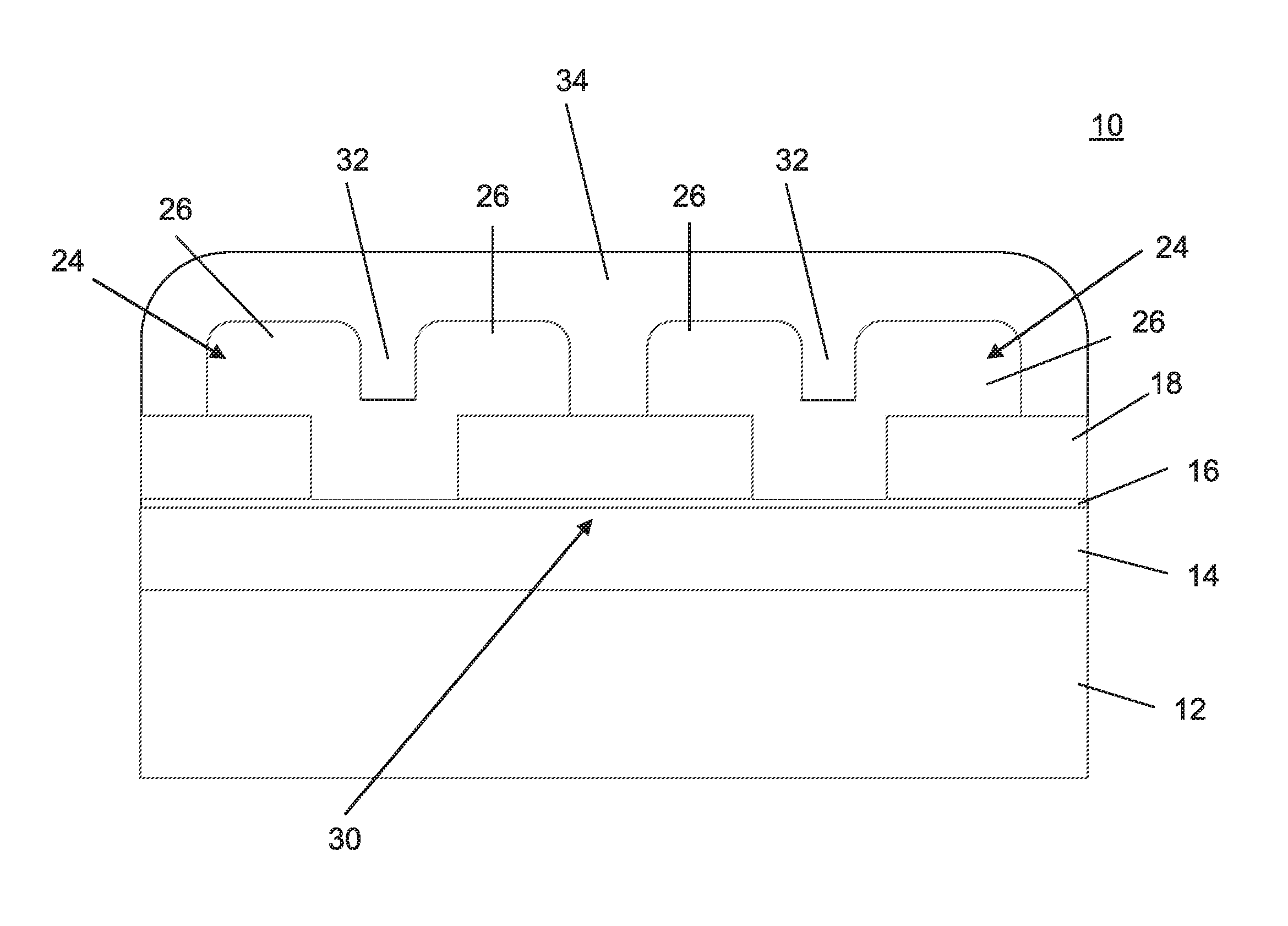
[0018]In accordance with the present principles, devices and methods for making the devices are provided to address the oxidation problem that leads to low-yield and unstable n-type field effect transistors (NFETs) in device fabrication with carbon nanotubes (CNT). In useful embodiments, a protective pattern forms metal contacts over its sidewalls to protect metal contacts for CNT NFETs from oxidation. While different materials may be employed form the protective pattern, in one embodiment, the protective pattern includes hydrogen silsesquioxane (HSQ), which can be reduced to silicon oxide after e-beam exposure. An overlapping portion of the metal contacts may is formed over the protective pattern and employed to further protect the metal contacts to from oxidation.

[0019]While CNT p-type metal contacts include inert Pd, n-type metal contacts including Sc or Er react with oxygen and suffer from severe degradation leading to low-yield and unstable NFETs. In accordance with the present...


PUM


Abstract

A field effect transistor includes a substrate and a gate dielectric formed on the substrate. A channel material is formed on the dielectric layer. The channel material includes carbon nanotubes. A patterned resist layer has openings formed therein. Metal contacts are formed on the channel material in the openings in the patterned resist layer and over portions of the patterned resist layer to protect sidewalls of the metal contacts to prevent degradation of the metal contacts.

Description

BACKGROUND[0001]Technical Field[0002]The present invention relates to transistor devices, and more particularly to carbon nanotube transistors with protected metal contacts.[0003]Description of the Related Art[0004]Among all the candidate materials for post-silicon era, carbon nanotubes (CNTs) have intrinsic ultra-thin body and exceptional electrical properties (high on current, superior current on / off ratio, long mean-free-path for ballistic transport, etc.), which makes them one of the most promising candidates for sub-10 nm technology node in semiconductor industry. The implementation of CNT-based complementary metal oxide semiconductor (CMOS) technology with low standby power dissipation requires both robust high-performance n-type field effect transistors (NFETs) and p-type field effect transistors (PFETs), which are usually realized by using low- and high-work function metal contacts to the intrinsic (undoped) CNT channel, respectively.[0005]While CNT p-type metal contacts (ty...

Claims


Application Information

Patent Timeline
IPC IPC(8): H01L51/00H01L51/05
CPCH01L51/0558H01L51/002H01L51/0048H10K71/621H10K85/221H10K10/84H10K10/466H10K2102/00H10K10/88H10K10/484H10K71/30H10K71/60
Inventor HAN, SHU-JENTANG, JIANSHI
Owner IBM CORP
Why Eureka
Try Eureka