Semiconductor device and manufacturing method thereof

a semiconductor and semiconductor technology, applied in the direction of semiconductor devices, electrical devices, transistors, etc., can solve the problems of low power consumption of the display device in which the transistor includes an oxide semiconductor is used, and achieve the effects of low leakage current, high frequency characteristics, and stable electrical characteristics

Active Publication Date: 2017-05-16
SEMICON ENERGY LAB CO LTD
View PDF187 Cites 10 Cited by
  • Summary
  • Abstract
  • Description
  • Claims
  • Application Information

AI Technical Summary

Benefits of technology

[0012]An object is to provide a transistor with stable electrical characteristics. Another object is to provide a transistor having a low leakage current in an off state. Another object is to provide a transistor with high frequency characteristics. Another object is to provide a transistor having a high on-state current. Another object is to provide a transistor with normally-off electrical characteristics. Another object is to provide a transistor with a small subthreshold swing value. Another object is to provide a highly reliable transistor.
[0023]A transistor with stable electrical characteristics can be provided. A transistor having a low leakage current in an off state can be provided. A transistor with high frequency characteristics can be provided. A transistor having a high on-state current can be provided. A transistor with normally-off electrical characteristics can be provided. A transistor with a small subthreshold swing value can be provided. A highly reliable transistor can be provided.

Problems solved by technology

For example, a display device in which a transistor including an oxide semiconductor is used is known to have low power consumption.

Method used


Image

  • Semiconductor device and manufacturing method thereof
  • Semiconductor device and manufacturing method thereof
  • Semiconductor device and manufacturing method thereof

Examples


embodiment 1

(Embodiment 1)

[0096]In this embodiment, structures of semiconductor devices of embodiments of the present invention will be described with reference to FIGS. 1A to 1C, FIGS. 2A and 2B, FIGS. 3A to 3D, FIGS. 4A to 4D, FIGS. 5A and 5B, FIGS. 6A to 6C, FIGS. 7A to 7D, and FIGS. 8A to 8C.

[0097]Structures of transistors, which are examples of the semiconductor devices of embodiments of the present invention, will be described below.

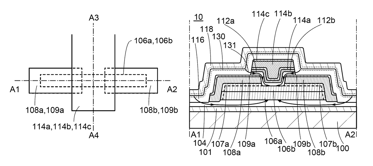
[0098]A structure of a transistor 10 will be described with reference to FIGS. 1A to 1C. FIG. 1A is a top view of the transistor 10. FIG. 1B is a cross-sectional view taken along dashed-dotted line A1-A2 in FIG. 1A. FIG. 1C is a cross-sectional view taken along dashed-dotted line A3-A4 in FIG. 1A. A region along dashed-dotted line A1-A2 shows a structure of the transistor 10 in the channel length direction, and a region along dashed-dotted line A3-A4 shows a structure of the transistor 10 in the channel width direction. The channel length direction of a transi...

embodiment 2

(Embodiment 2)

[0275]In this embodiment, a method for manufacturing the semiconductor device of one embodiment of the present invention will be described with reference to FIGS. 9A to 9F, FIGS. 10A to 10F, FIGS. 11A to 11D, and FIGS. 12A to 12J.

[0276]A method for manufacturing the transistor 10 will be described below with reference to FIGS. 9A to 9F, FIGS. 10A to 10F, and FIGS. 11A to 11D.

[0277]First, the substrate 100 is prepared. Any of the above-mentioned substrates can be used for the substrate 100.

[0278]Next, the insulator 101 is formed. Any of the above-mentioned insulators can be used for the insulator 101.

[0279]The insulator 101 may be formed by a sputtering method, a chemical vapor deposition (CVD) method, a molecular beam epitaxy (MBE) method, a pulsed laser deposition (PLD) method, an atomic layer deposition (ALD) method, or the like.

[0280]CVD methods can be classified into a plasma enhanced CVD (PECVD) method using plasma, a thermal CVD (TCVD) method using heat, a photo ...

embodiment 3

(Embodiment 3)

[0467]In this embodiment, the oxide semiconductor included in a semiconductor device of one embodiment of the present invention will be described in detail below.

[0468]A structure of an oxide semiconductor will be described below.

[0469]An oxide semiconductor is classified into a single crystal oxide semiconductor and a non-single-crystal oxide semiconductor. Examples of a non-single-crystal oxide semiconductor include a c-axis aligned crystalline oxide semiconductor (CAAC-OS), a polycrystalline oxide semiconductor, a nanocrystalline oxide semiconductor (nc-OS), an amorphous-like oxide semiconductor (a-like OS), and an amorphous oxide semiconductor.

[0470]From another perspective, an oxide semiconductor is classified into an amorphous oxide semiconductor and a crystalline oxide semiconductor. Examples of a crystalline oxide semiconductor include a single crystal oxide semiconductor, a CAAC-OS, a polycrystalline oxide semiconductor, and an nc-OS.

[0471]It is known that an ...


PUM


Abstract

Provided is a transistor with stable electrical characteristics. Provided is a semiconductor device including an oxide semiconductor over a substrate, a first conductor in contact with a top surface of the oxide semiconductor, a second conductor in contact with the top surface of the oxide semiconductor, a first insulator over the first and second conductors and in contact with the top surface of the oxide semiconductor, a second insulator over the first insulator, a third conductor over the second insulator, and a third insulator over the third conductor. The third conductor overlaps with the first conductor with the first and second insulators positioned therebetween, and overlaps with the second conductor with the first and second insulators positioned therebetween. The first insulator contains oxygen. The second insulator transmits less oxygen than the first insulator. The third insulator transmits less oxygen than the first insulator.

Description

BACKGROUND OF THE INVENTION[0001]1. Field of the Invention[0002]The present invention relates to, for example, a transistor or a semiconductor device. The present invention relates to, for example, a method for manufacturing a transistor or a semiconductor device. The present invention relates to, for example, a display device, a light-emitting device, a lighting device, a power storage device, a memory device, a processor, or an electronic device. The present invention relates to a method for manufacturing a display device, a liquid crystal display device, a light-emitting device, a memory device, or an electronic device. The present invention relates to a driving method of a display device, a liquid crystal display device, a light-emitting device, a memory device, or an electronic device.[0003]Note that one embodiment of the present invention is not limited to the above technical field. The technical field of one embodiment of the invention disclosed in this specification and the ...

Claims


Application Information

Patent Timeline
Patent Type & Authority Patents(United States)
IPC IPC(8): H01L29/786H01L29/06H01L29/51
CPCH01L29/7869H01L29/0607H01L29/513H01L29/517H01L29/66969H01L29/42384H01L29/4908H01L27/1207H01L27/1225
Inventor YAMAZAKI, SHUNPEITANAKA, TETSUHIROSHIMOMURA, AKIHISATOKUMARU, RYOYAMANE, YASUMASASATO, YUHEIOKUNO, NAOKINAKASHIMA, MOTOKI
Owner SEMICON ENERGY LAB CO LTD
Why Eureka
Try Eureka