

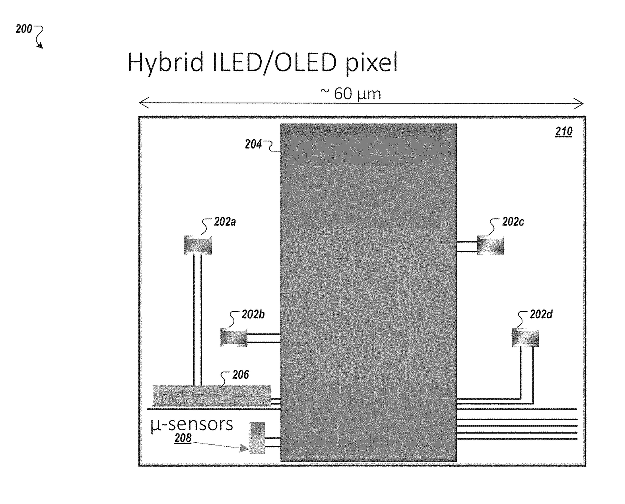
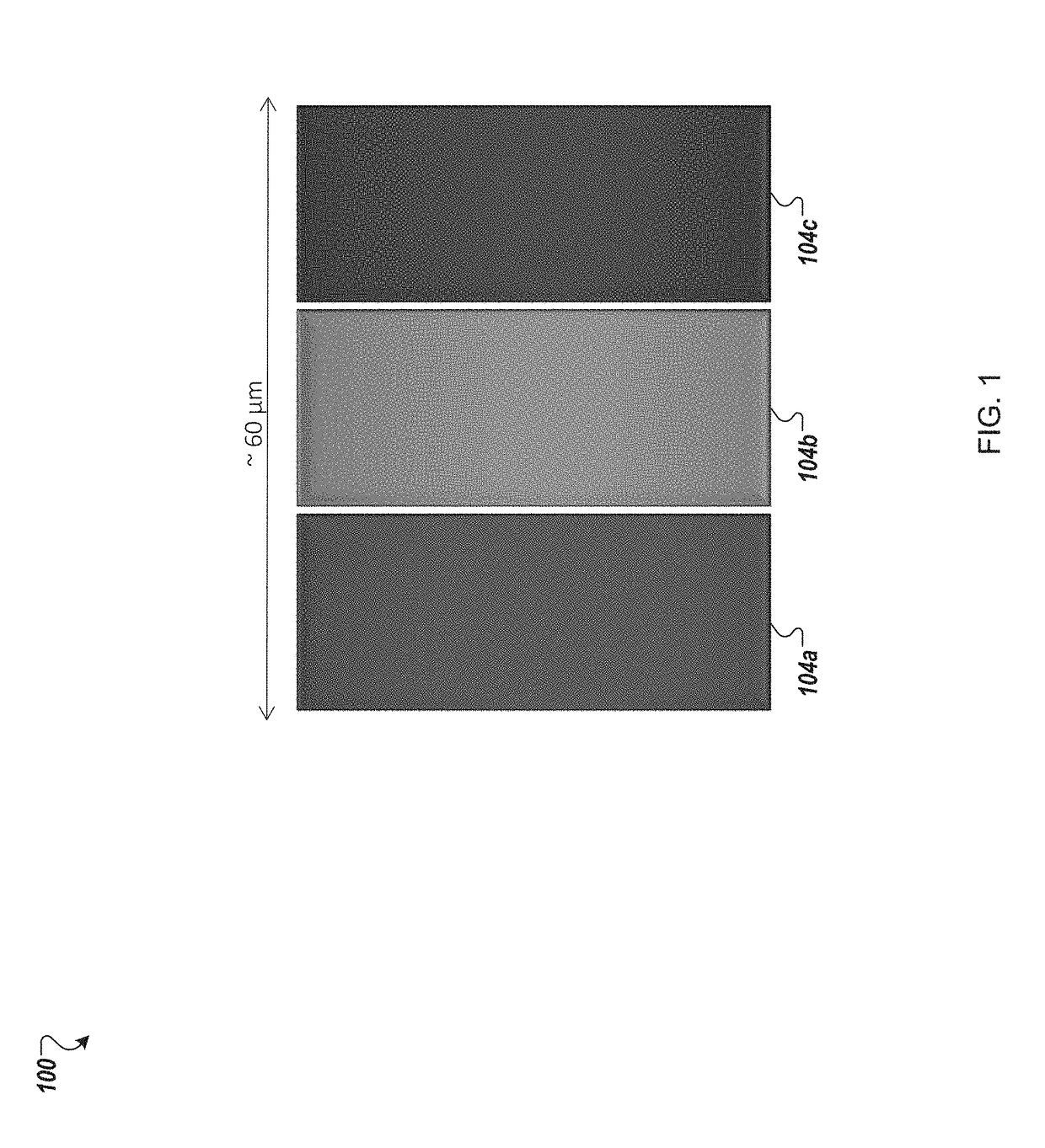
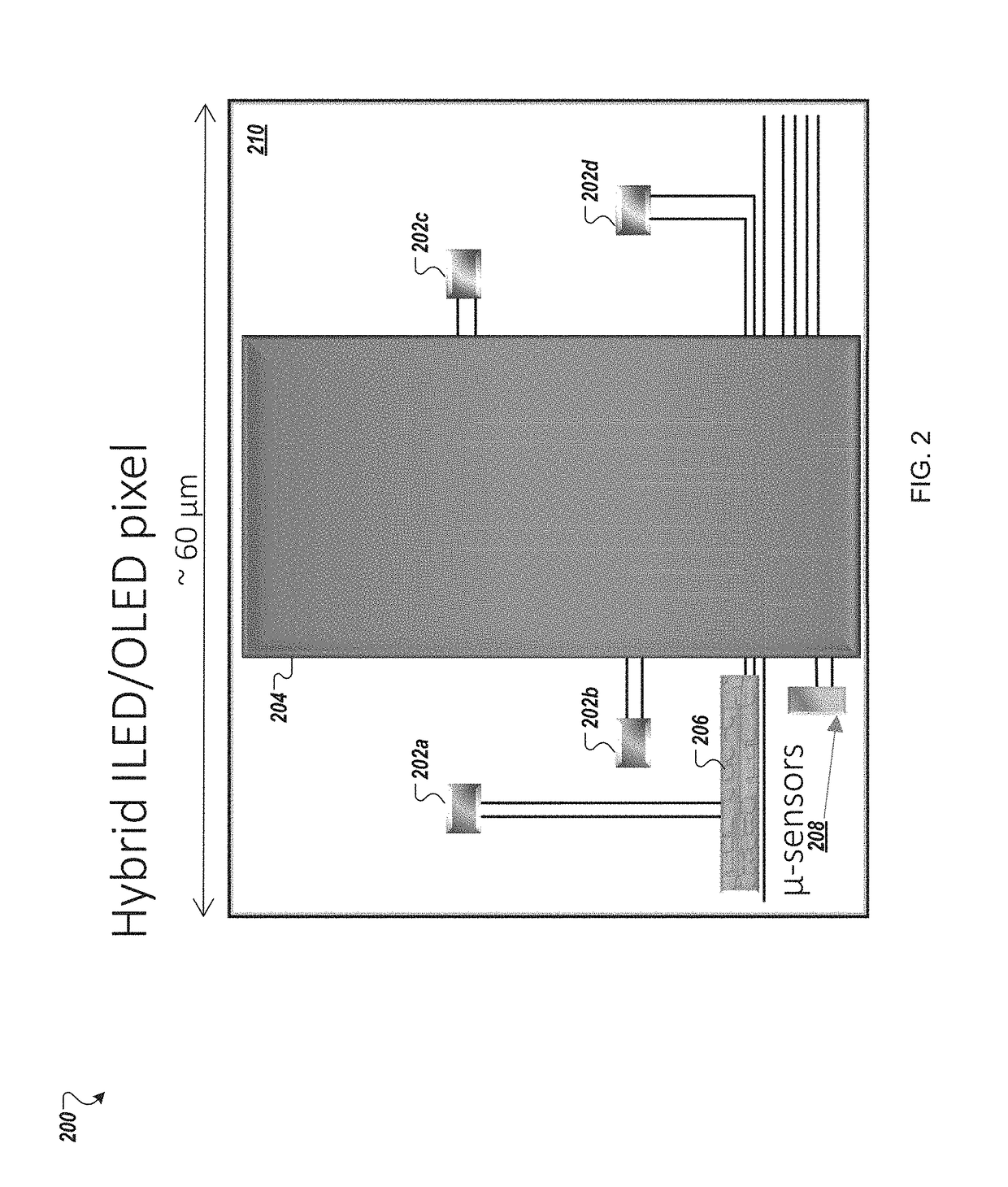
Micro assembled hybrid displays and lighting elements
a hybrid display and lighting element technology, applied in the field of displays, can solve the problems of limited viewing angle, green leds suffer from the “green gap”, a portion of the light spectrum where the efficiency of green leds is plummeting, etc., to achieve the effect of enhancing the manufacturability of utilizing, optimizing color quality, and improving the manufacturing yield of displays
- Summary
- Abstract
- Description
- Claims
- Application Information
AI Technical Summary
Benefits of technology
Problems solved by technology
Method used
Image

Examples
Embodiment Construction
[0123]As used herein the expression “semiconductor element” and “semiconductor structure” are used synonymously and broadly refer to a semiconductor material, structure, device, or component of a device. Semiconductor elements include high-quality single crystalline and polycrystalline semiconductors, semiconductor materials fabricated via high-temperature processing, doped semiconductor materials, organic and inorganic semiconductors, and composite semiconductor materials and structures having one or more additional semiconductor components and / or non-semiconductor components, such as dielectric layers or materials and / or conducting layers or materials. Semiconductor elements include semiconductor devices and device components including, but not limited to, transistors, photovoltaics including solar cells, diodes, light-emitting diodes, lasers, p-n junctions, photodiodes, integrated circuits, and sensors. In addition, semiconductor element can refer to a part or portion that forms ...
PUM
 Abstract
Description
Claims
Application Information