Tunable semiconductor laser based on reconstruction-equivalent chirp and series mode or series and parallel hybrid integration, and preparation thereof
a semiconductor laser and reconstruction equivalent technology, applied in semiconductor laser arrangements, semiconductor lasers, lasers, etc., can solve problems such as fragile laser bars
- Summary
- Abstract
- Description
- Claims
- Application Information
AI Technical Summary
Benefits of technology
Problems solved by technology
Method used
Image
Examples
first embodiment
conductor Laser Based on REC Technique and Series Configuration Working in 1550 nm Window
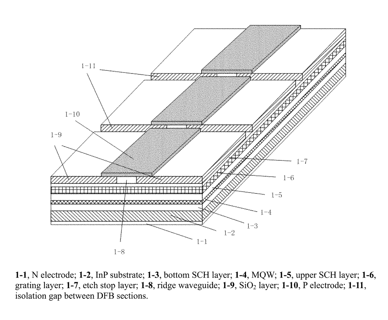
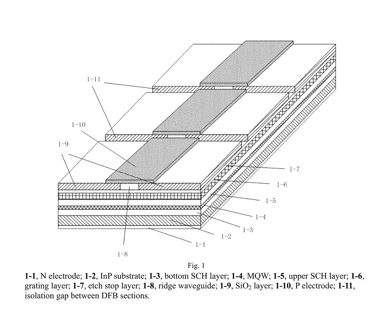
[0025]As shown in FIG. 1, the epitaxy is grown on an n-type InP (100) substrate by metal organic vapor phase epitaxy (MOVPE). The first growth comprises of a 200 nm n-type InP buffer layer, a 100 nm lattice-matched InGaAsP waveguide layer, strained InGaAsP multiple-quantum-well (MQW) layers with photoluminescence wavelength of 1.53 um, and a 70 nm InGaAsP grating layer. Then uniform grating are fabricated on the grating layer, after which the sampling patterns are transferred to the grating by conventional photolithography. Then in the second growth step, a 100 nm p-type lattice-matched InGaAsP waveguide layer, a 1.7 um p-type InP layer and a 100 nm p-type InGaAs contact layer are grown successively. Then the contact layer in the isolation region between two DFB sections is removed and ion implanting is performed. After that, the ridge waveguide is patterned and a 200 nm SiO2 layer is deposited ...
second embodiment
onductor Laser Based on REC Technique and Series / Parallel Configuration Working in 1550 nm Window
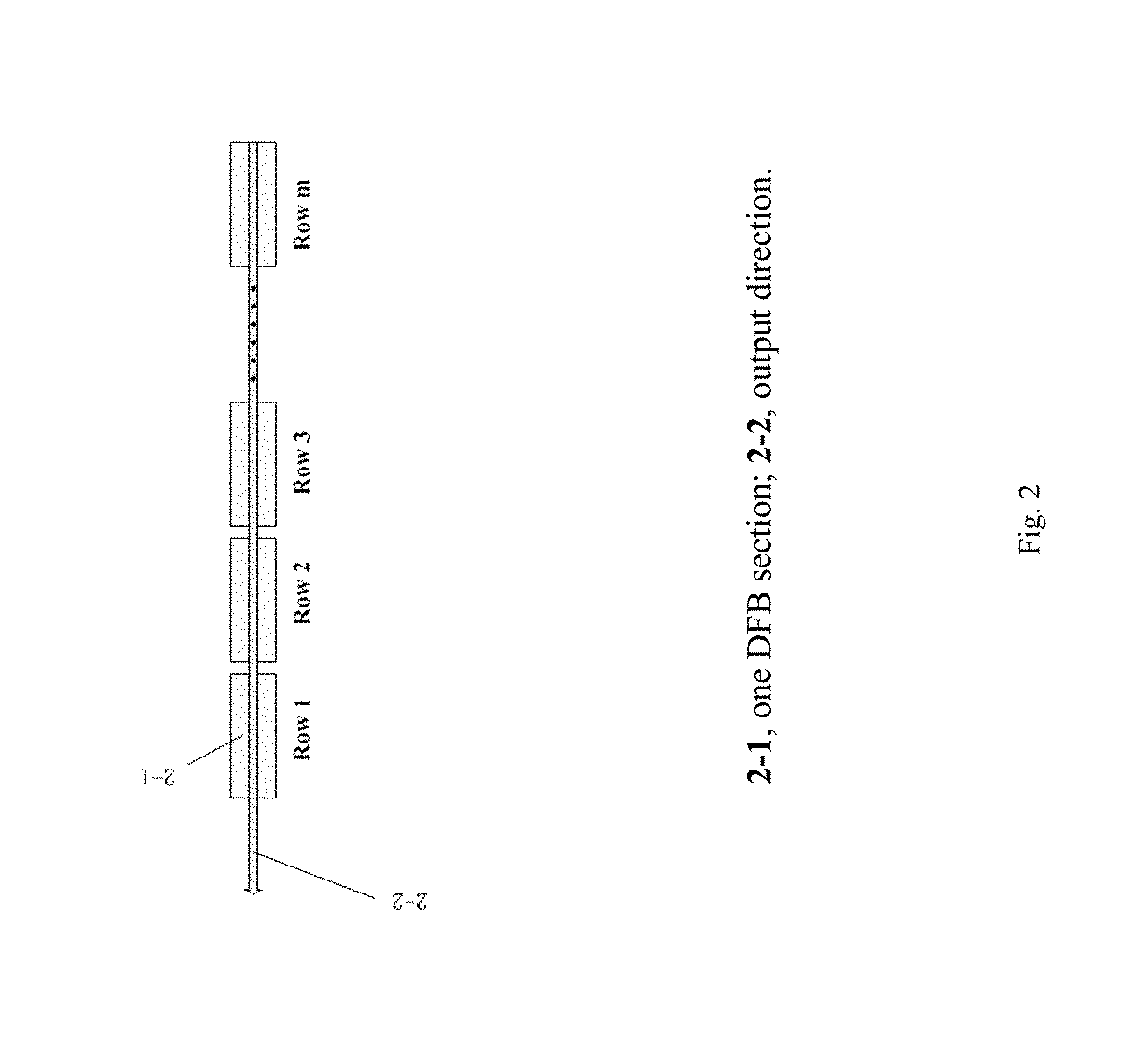
[0026]As shown in FIG. 2, the epitaxy is grown on an n-type InP (100) substrate by metal organic vapor phase epitaxy (MOVPE). The first growth comprises of a 200 nm n-type InP buffer layer, a 100 nm lattice-matched InGaAsP waveguide layer, strained InGaAsP multiple-quantum-well (MQW) layers with photoluminescence wavelength of 1.53 um, and a 70 nm InGaAsP grating layer. Then uniform grating are fabricated on the grating layer, after which the sampling patterns are transferred to the grating by conventional photolithography. Then in the second growth step, a 100 nm p-type lattice-matched InGaAsP waveguide layer, a 1.7 um p-type InP layer and a 100 nm p-type InGaAs contact layer are grown successively. Then the contact layer in the isolation region between two DFB sections is removed and ion implanting is performed. After that, the ridge waveguide is patterned and a 200 nm SiO2 layer is de...
PUM
 Abstract
Description
Claims
Application Information


