Tunable semiconductor laser based on reconstruction-equivalent chirp and series mode or series and parallel hybrid integration, and preparation thereof

a semiconductor laser and reconstruction equivalent technology, applied in semiconductor laser arrangements, semiconductor lasers, lasers, etc., can solve problems such as fragile laser bars

Active Publication Date: 2016-05-12
NANJING HUAFEI OPTOELECTRONICS TECH CO LTD
View PDF3 Cites 4 Cited by
  • Summary
  • Abstract
  • Description
  • Claims
  • Application Information

AI Technical Summary

Benefits of technology

[0013]The object of the present invention is to provide a method by which low-cost tunable lasers can be fabricated by holographic exposure combining with conventional photolithography. Two approaches are proposed: series configuration and hybrid series / parallel configuration. These kinds of tunable lasers can be used in WDM-PON optical communication systems.

Problems solved by technology

Because the laser material is brittle, the laser bar is fragile when the laser cavity is very long.

Method used


Image

  • Tunable semiconductor laser based on reconstruction-equivalent chirp and series mode or series and parallel hybrid integration, and preparation thereof
  • Tunable semiconductor laser based on reconstruction-equivalent chirp and series mode or series and parallel hybrid integration, and preparation thereof
  • Tunable semiconductor laser based on reconstruction-equivalent chirp and series mode or series and parallel hybrid integration, and preparation thereof

Examples


first embodiment

conductor Laser Based on REC Technique and Series Configuration Working in 1550 nm Window

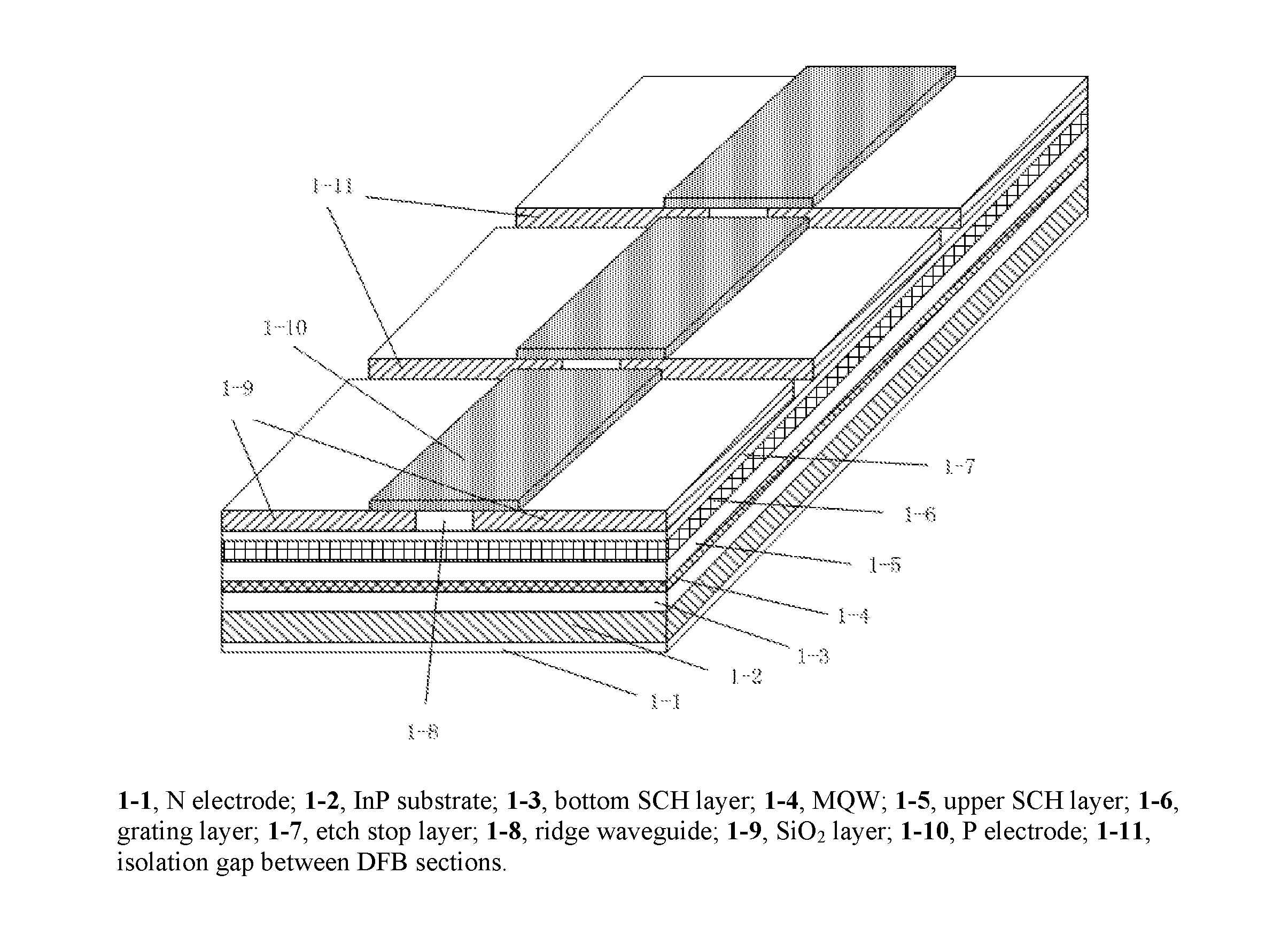
[0024]As shown in FIG. 1, the epitaxy is grown on an n-type InP (100) substrate by metal organic vapor phase epitaxy (MOVPE). The first growth comprises of a 200 nm n-type InP buffer layer, a 100 nm lattice-matched InGaAsP waveguide layer, strained InGaAsP multiple-quantum-well (MQW) layers with photoluminescence wavelength of 1.53 um, and a 70 nm InGaAsP grating layer. Then uniform grating are fabricated on the grating layer, after which the sampling patterns are transferred to the grating by conventional photolithography. Then in the second growth step, a 100 nm p-type lattice-matched InGaAsP waveguide layer, a 1.7 um p-type InP layer and a 100 nm p-type InGaAs contact layer are grown successively. Then the contact layer in the isolation region between two DFB sections is removed and ion implanting is performed. After that, the ridge waveguide is patterned and a 200 nm SiO2 layer is deposited ...

second embodiment

onductor Laser Based on REC Technique and Series / Parallel Configuration Working in 1550 nm Window

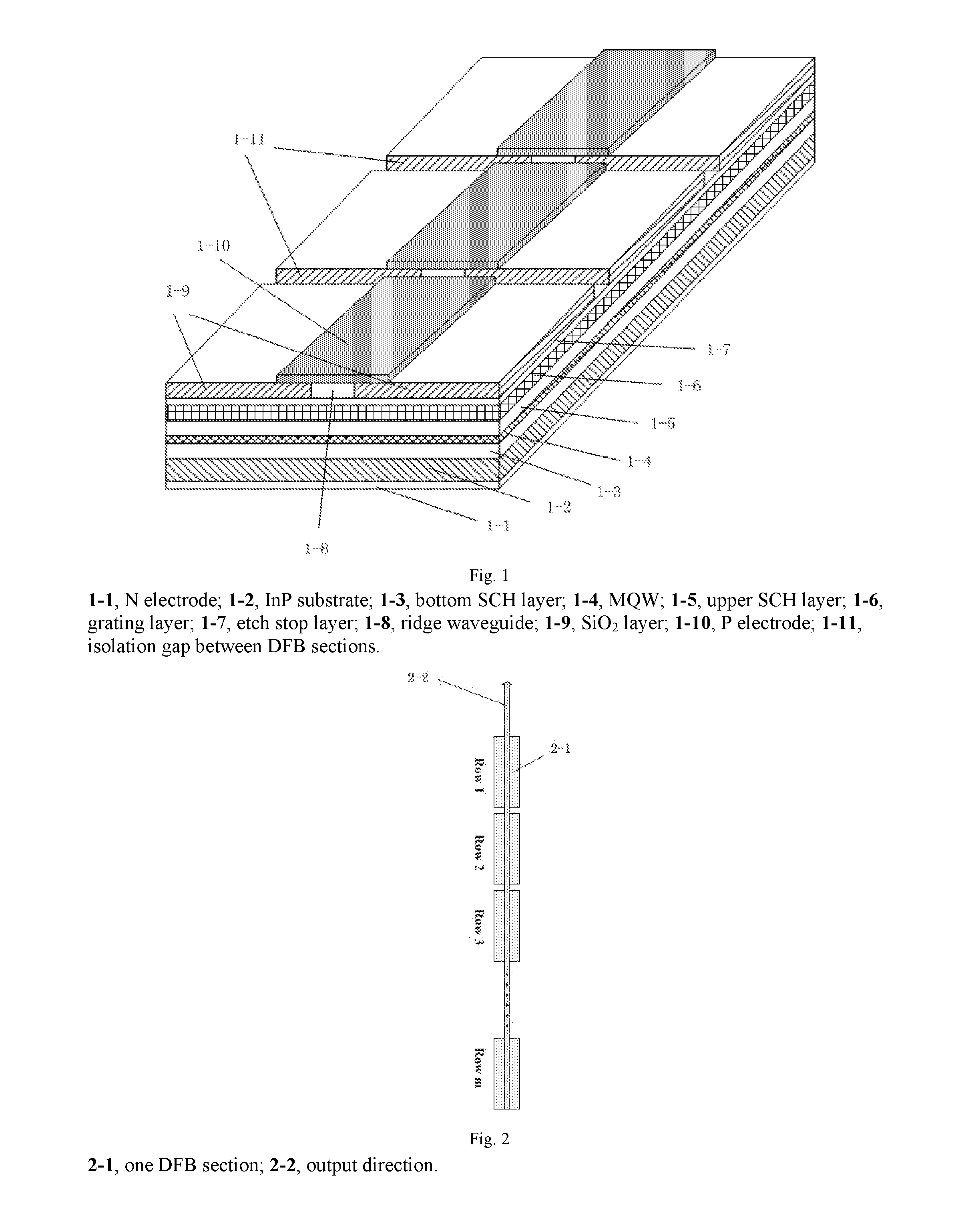
[0025]As shown in FIG. 2, the epitaxy is grown on an n-type InP (100) substrate by metal organic vapor phase epitaxy (MOVPE). The first growth comprises of a 200 nm n-type InP buffer layer, a 100 nm lattice-matched InGaAsP waveguide layer, strained InGaAsP multiple-quantum-well (MQW) layers with photoluminescence wavelength of 1.53 um, and a 70 nm InGaAsP grating layer. Then uniform grating are fabricated on the grating layer, after which the sampling patterns are transferred to the grating by conventional photolithography. Then in the second growth step, a 100 nm p-type lattice-matched InGaAsP waveguide layer, a 1.7 um p-type InP layer and a 100 nm p-type InGaAs contact layer are grown successively. Then the contact layer in the isolation region between two DFB sections is removed and ion implanting is performed. After that, the ridge waveguide is patterned and a 200 nm SiO2 layer is de...


PUM


Abstract

A tunable distributed feedback (DFB) semiconductor laser based on a series mode or a series and parallel hybrid mode. A grating structure of the laser is a sampling Bragg grating based on the reconstruction-equivalent chirp technology. DFB lasers with different operating wavelengths based on the reconstruction-equivalent chirp technology are integrated together by a sampling series combination mode or a series/parallel hybrid mode, one of the lasers is selected to operate via a current, and the operating wavelength of the laser can be controlled by adjusting the current or the temperature, so that the continuous tuning of the operating wavelengths of the lasers can be realized. Various wavelength signals in parallel channels are coupled and then output from the same waveguide. An electrical isolation area (1-11) is adopted between lasers connected in series or lasers connected in series and connected in parallel to reduce the crosstalk between adjacent lasers.

Description

TECHNICAL FIELD[0001]The present invention relates to optical components for telecommunications and, more particularly, to the design and manufacture method of low-cost tunable distributed feedback (DFB) semiconductor lasers based on reconstruction equivalent chirp (REC) technique.BACKGROUND OF THE INVENTION[0002]During the last two decades, the increasing demand for communication bandwidth boosted the development of fiber-optical communications. A number of methods dedicated to increase the capacity and bandwidth are proposed, in which dense wavelength division multiplexing (DWDM) is attractive and has been exploited due to its flexibility to upgrade or reconstruct on the basis of existing infrastructures.[0003]DWDM technology can be used to increase the transmission capacity of a system by increasing the number of wavelengths. For instance, 80 or 100 channels with different signals can be transmitted through a single fiber at the same time, and then can be separated when they reac...

Claims


Application Information

Patent Timeline
Patent Type & Authority Applications(United States)
IPC IPC(8): H01S5/125H01S5/06H01S5/40H01S5/34H01S5/343H01S5/028H01S5/12H01S5/10
CPCH01S5/125H01S5/1212H01S5/0612H01S5/4025H01S5/3403H01S5/3434H01S5/0287H01S5/1096H01S5/1209H01S5/4006H01S5/4087H01S5/026H01S5/4012
Inventor LI, LIANYANTANG, SONGCHEN, XIANGFEIZHANG, YUNSHANLU, JUN
Owner NANJING HUAFEI OPTOELECTRONICS TECH CO LTD
Why Eureka
Try Eureka