Supercharge Your Innovation With Domain-Expert AI Agents!

Method for manufacturing circuit board

a manufacturing method and circuit board technology, applied in the field of manufacturing circuit boards, can solve the problems of circuit boards failing to perform normal functions, line width/pitch of connection circuits that need to be smaller, and current equipment and processes for mass production encounter tough challenges, so as to improve electrical quality, the processing steps of the method are simple, and the effect of improving electrical quality

Active Publication Date: 2017-08-29
KINSUS INTERCONNECT TECH
View PDF4 Cites 0 Cited by
  • Summary
  • Abstract
  • Description
  • Claims
  • Application Information

AI Technical Summary

Benefits of technology

The present invention provides a method for manufacturing a circuit board with fine line width / pitch to improve the precision of the electrical circuit. The method can manufacture the circuit board having fine line width / pitch less than 10 μm to greatly improve the electrical quality. The processing steps of the method are simple and easy to implement, and the manufacturing cost is reduced, thereby providing the advantage of lower cost and meeting the requirements of fine line width / pitch by the application field of packaging electronic devices in consuming electronic products.

Problems solved by technology

As a result, the line width / pitch of the connection circuit needs smaller size, and the current equipments and processes for mass production encounter tough challenge.
However, for the line width / pitch about 10-20 μm, roughness Rz of the copper layer should be about 2 μm, or otherwise the circuit pattern is easily distorted to cause the circuit board to fail to normal function.
However, one of the shortcomings for the above methods in the prior arts is that the remaining resin is not stable after the PCF is removed such that the circuit pattern layer formed by the chemical plating process is easy to break, peel off due to weak adhesion.
It is thus difficult to prevent the portion of the circuit patter layer filling up the blind holes as connection plug with a vertical shape from being shifted or distorted.
As a result, the electrical property and reliability of the electrical circuit of the circuit board are adversely affected.

Method used


Image

  • Method for manufacturing circuit board
  • Method for manufacturing circuit board
  • Method for manufacturing circuit board

Examples


Embodiment Construction

[0023]The accompanying drawings are included to provide a further understanding of the invention, and are incorporated in and constitute a part of this specification. The drawings illustrate embodiments of the invention and, together with the description, serve to explain the principles of the invention.

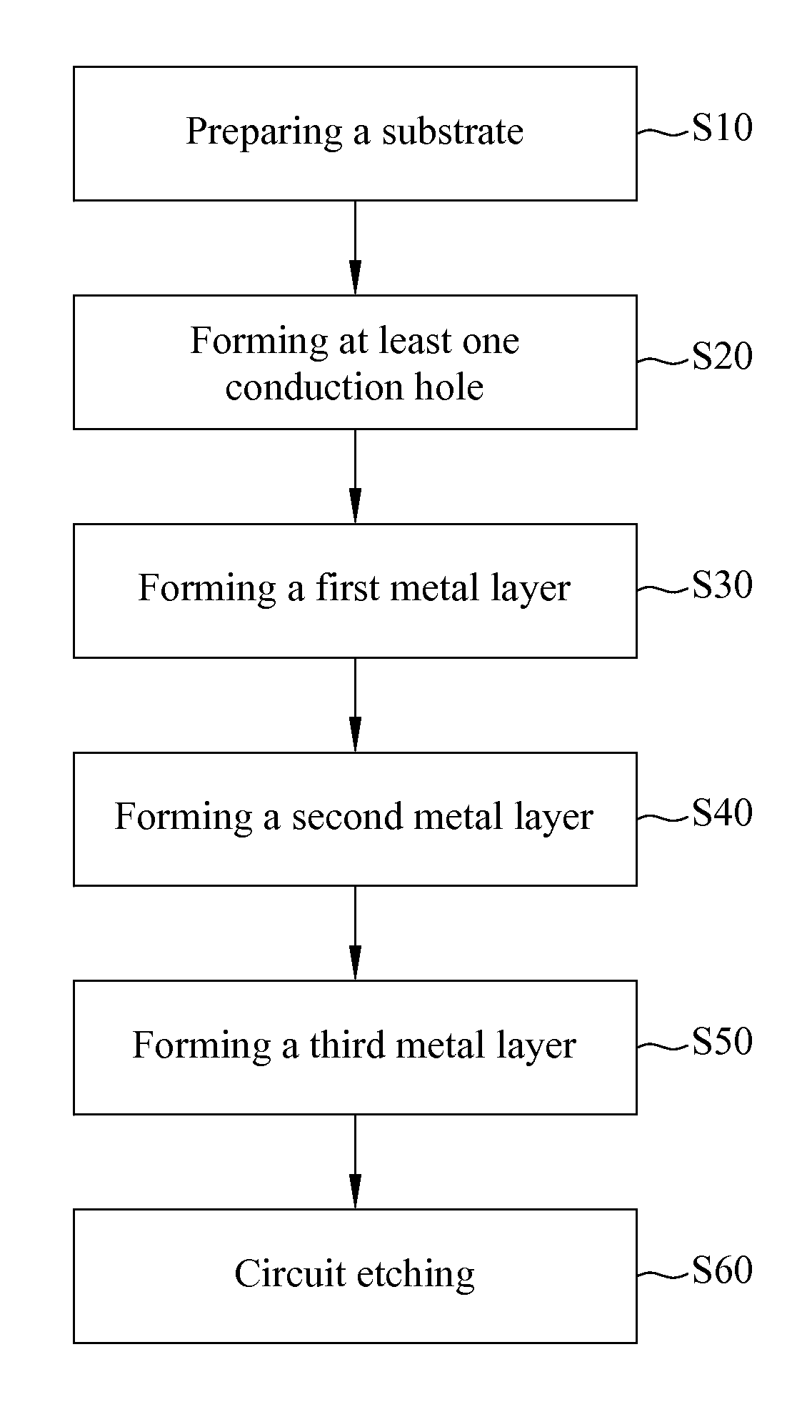
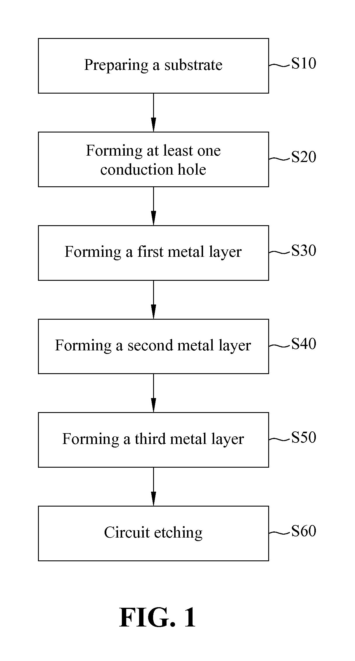
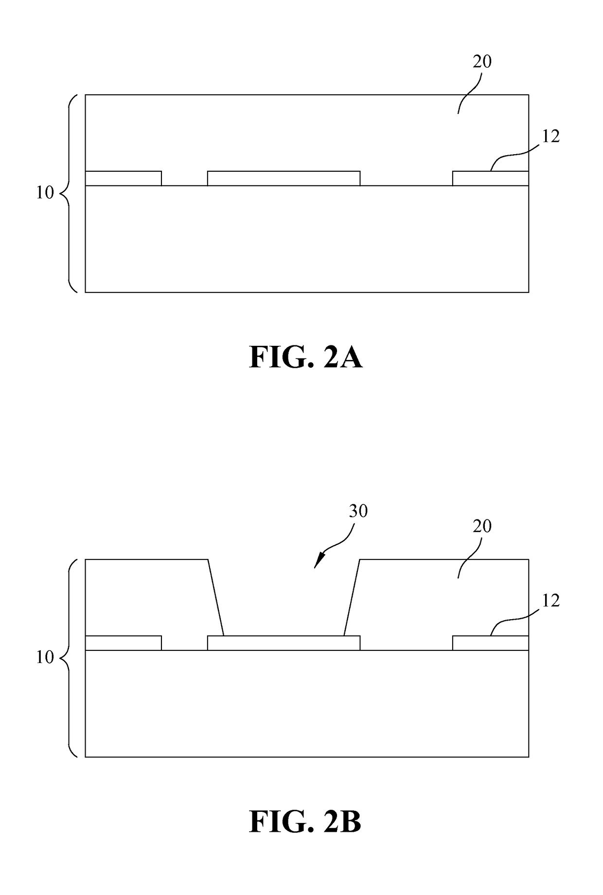
[0024]Please refer to FIG. 1 illustrating the processing steps of the method for manufacturing a circuit board according to the first embodiment of the present invention. As shown in FIG. 1, the method of the first embodiment generally comprises the processing steps S10, S20, S24, S30, S40, S50 and S60, which are sequentially performed for manufacturing the circuit board with fine line width / pitch. Additionally, to further clearly understand the technical characteristics of the present invention, refer to FIGS. 2A to 2F, which are schematic views illustrating the respective processing steps of the method of the first embodiment of the present invention.

[0025]First, the method of the ...


PUM

PropertyMeasurementUnit
widthaaaaaaaaaa
widthaaaaaaaaaa
roughness Rzaaaaaaaaaa

Abstract

Disclosed is a method for manufacturing a circuit board, including preparing a substrate having a resin layer and a stop layer, forming at least one conduction hole penetrating the resin layer and stopping at the stop layer, forming a first metal layer through a sputtering process, forming a second metal layer on the first metal layer through a chemical plating process, forming a third metal layer having a circuit pattern, exposing part of the second metal layer and filling up the conduction hole through an electroplating process, and etching the second metal layer and the first metal layer under the second metal layer to expose the resin layer under the first metal layer. Since the first metal layer provides excellent surface properties, the second and third metal layers are well fixed and stable. The etched circuit pattern has a line width / pitch less than 10 μm for fine line width / pitch.

Description

BACKGROUND OF THE INVENTION[0001]1. Field of the Invention[0002]The present invention generally relates to a method for manufacturing a circuit board, and more specifically to a method for manufacturing a circuit board comprising a sputtering process, a chemical plating process and an electroplating process sequentially performed to form a first metal layer on a substrate, a second metal layer on the first metal layer and a third metal layer on the second metal layer, respectively, and further comprising a circuit etching process to form an electrical circuit with fine line width / pitch by etching the first and second metal layers.[0003]2. The Prior Arts[0004]Recently, as the technology of the VLSI (very large scale integrated circuit) made great progress, the connection circuit has become much smaller. For example, in the 22 nm semiconductor technology, both chip density and ability of signal processing are increasingly enhanced. As a result, the line width / pitch of the connection c...

Claims


Application Information

Patent Timeline
Patent Type & Authority Patents(United States)
IPC IPC(8): H05K3/46B23K26/402H05K3/42B23K26/382B23K103/00
CPCB23K26/402B23K26/389H05K3/426H05K3/4644B23K2203/30B23K2203/50H05K2201/0341B23K26/382B23K2101/40B23K2103/172B23K2103/42B23K2103/50B23K2103/30
Inventor LAN, JAEN-DONLIN, PIN-CHUNGTSENG, CHEN-RUIHO, CHENG-ENCHEN, YU-AN
Owner KINSUS INTERCONNECT TECH
Features
  • R&D
  • Intellectual Property
  • Life Sciences
  • Materials
  • Tech Scout
  • Unparalleled Data Quality
  • Higher Quality Content
  • 60% Fewer Hallucinations
Learn More