Semiconductor ferroelectric storage transistor and method for manufacturing same

a technology of ferroelectric storage transistor and semiconductor, which is applied in the direction of semiconductor devices, electrical equipment, basic electric elements, etc., can solve the problems of increasing the difficulty of the fabrication process, and the variation of the threshold voltage between the two states of the different fefets, etc., and achieve excellent data retention characteristics, excellent pulse rewrite endurance properties, and excellent characteristics

Active Publication Date: 2017-10-03
NAT INST OF ADVANCED IND SCI & TECH
View PDF6 Cites 2 Cited by
  • Summary
  • Abstract
  • Description
  • Claims
  • Application Information

AI Technical Summary

Benefits of technology

[0027]According to the present invention, it becomes possible to form an FeFET which has a broad memory window, excellent data retention characteristic, excellent pulse rewrite endurance property, etc. in a 200 nm or thinner ferroelectric thin film, so it becomes possible to realize an FeFET with excellent characteristics by a fine gate length of under 50 nm and in turn becomes possible to provide a low power consumption nonvolatile memory using highly-integrated FeFETs.

Problems solved by technology

If the thickness Li of the gate insulator with respect to Lg=1 μm is Li=400 nm, the aspect ratio of the cross-section of the gate insulator is a low A=Li / Lg=0.4 and there is little difficulty in the fabrication process such as the etching to form step differences and formation of a film covering step differences, but if becoming finer down to Lg=100 nm, Li=400 nm and A=4 result and the difficulty of the fabrication process increases.
When arranging a large number of FeFETs in an array to obtain a large scale integration memory, the variation in the two threshold voltages which correspond to the two states in the different FeFETs becomes a problem.

Method used


Image

  • Semiconductor ferroelectric storage transistor and method for manufacturing same
  • Semiconductor ferroelectric storage transistor and method for manufacturing same
  • Semiconductor ferroelectric storage transistor and method for manufacturing same

Examples


example 1

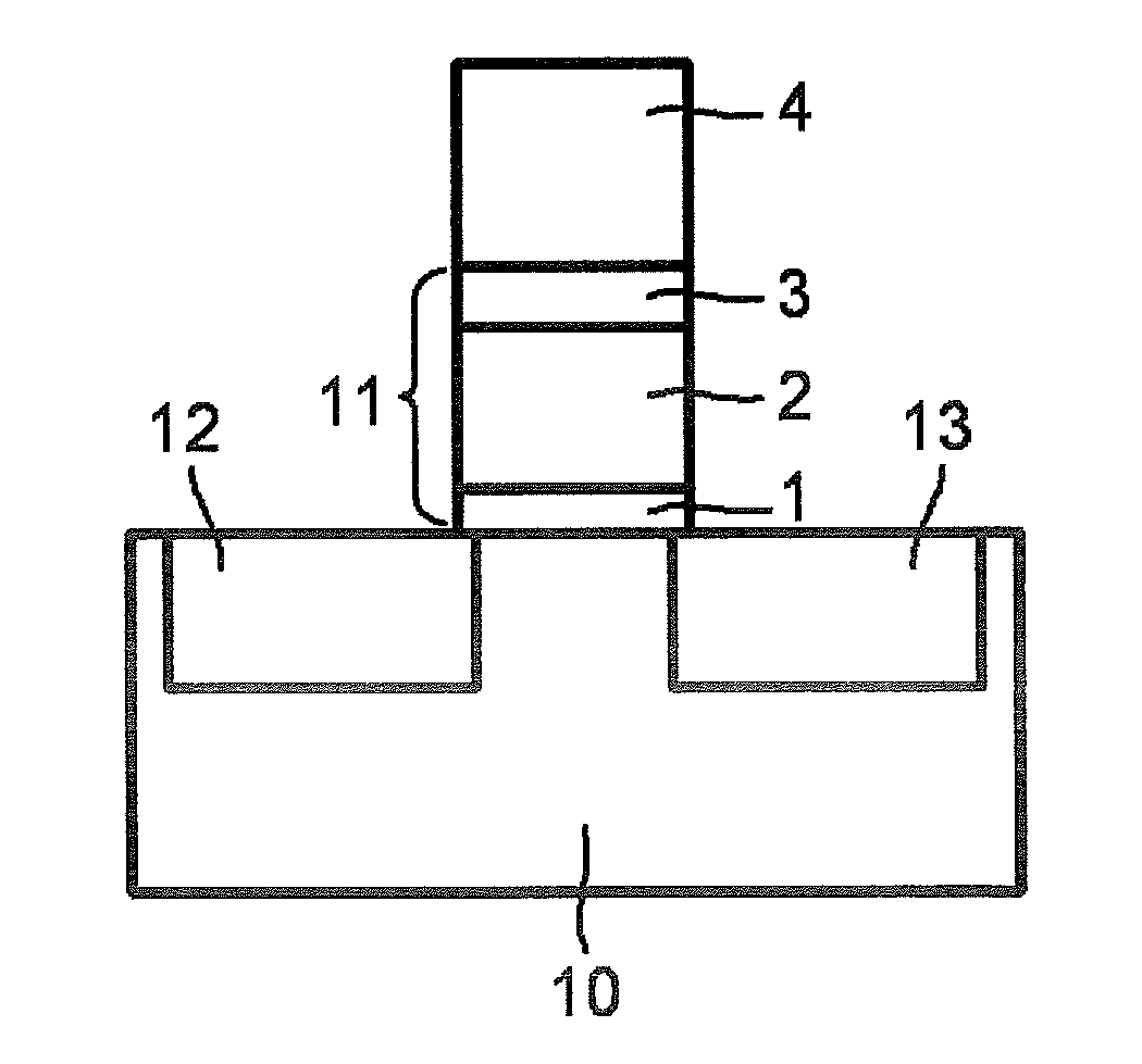
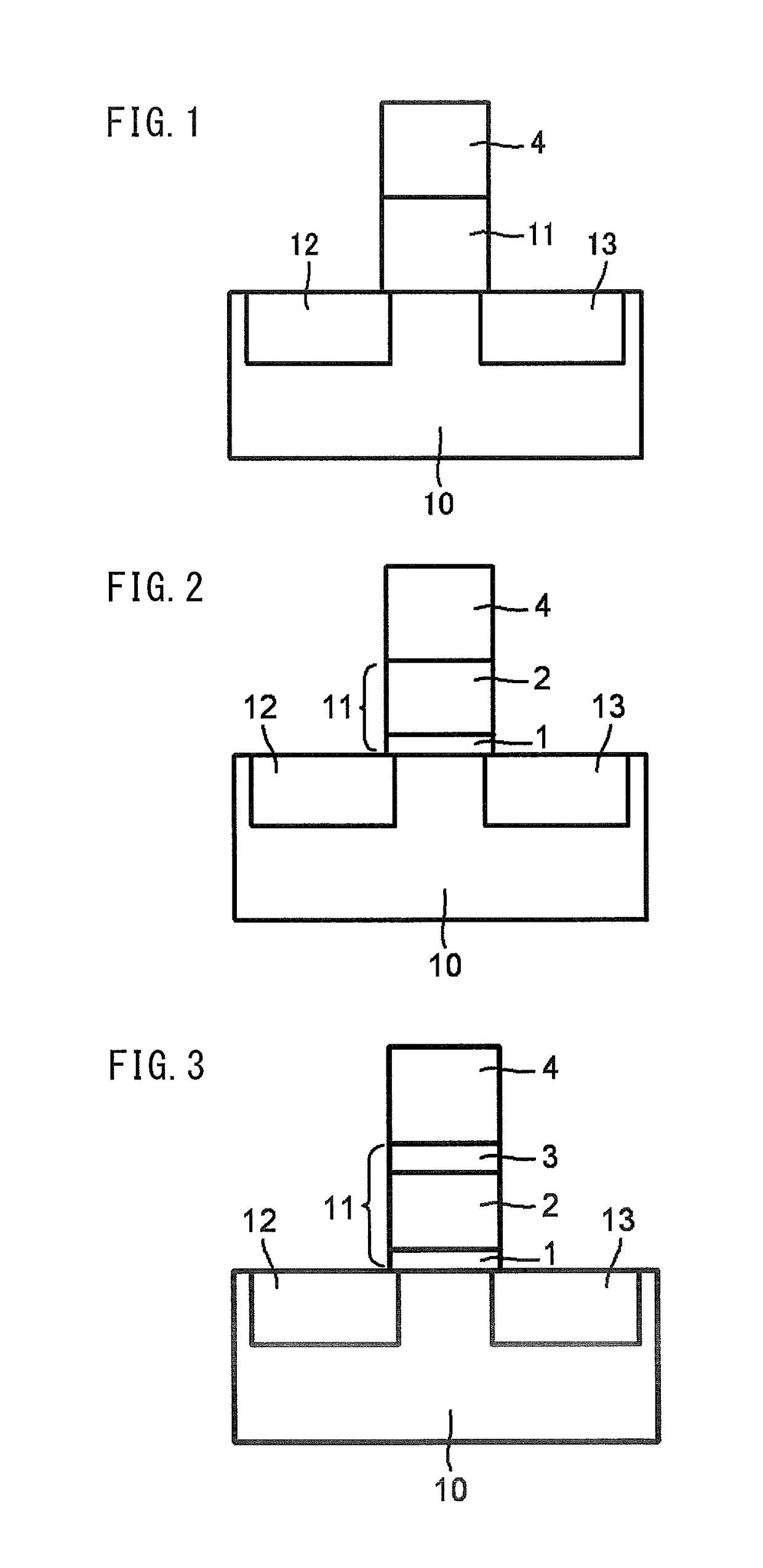
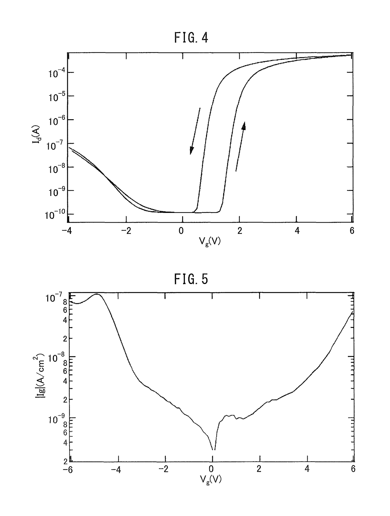
[0090]Example 1 relates to the second embodiment (see FIG. 2). A semiconductor body for an n-channel transistor made by a silicon material was used. The material of the first insulator was halfnium-aluminum oxide. The pulse laser deposition method was used. The target was comprised of Hf, Al, and O and the ratio of composition of Hf and Al was 3:2. The film thickness was 7 nm. The atmospheric gas during deposition was nitrogen and the pressure was 0.11 Torr. The temperature of the semiconductor body was 220° C. The second insulator was deposited by the pulse laser deposition method. The single target method was used. The target was comprised of strontium, calcium, bismuth, tantalum, and oxygen. Several targets changed in the ratio of composition of elements of strontium and calcium (Sr:Ca=1−x:x) were prepared. The ratio of composition of strontium, calcium, bismuth, and tantalum in the targets was set to Sr:Ca:Bi:Ta=1−x:x:3:2. The thickness y of the second insulator was changed in s...

example 2

[0093]Example 2 also relates to the second embodiment (see FIG. 2). A semiconductor body for an n-channel transistor which is formed by a silicon material was used. The material of the first insulator 1 was halfnium-aluminum oxide. The pulse laser deposition method was used. The target was comprised of Hf, Al, and O, and the ratio of composition of Hf and Al was 3:2. The film thickness was 7 nm. At the time of deposition, the atmospheric gas was nitrogen of a pressure of 0.11 Torr. The temperature of the semiconductor body was 220° C. The second insulator 2 was deposited by the pulse laser deposition method. The multiple target method was used and two targets were prepared. The first target was made of strontium, calcium, bismuth, tantalum, and oxygen with a ratio of composition of those elements of Sr:Ca:Bi:Ta=0.5:0.5:3:2, while the second target was comprised of strontium, bismuth, tantalum, and oxygen. The ratio of composition of the elements was Sr:Ca:Bi:Ta =1:0:3:2. The deposit...

example 3

[0098]Example 3 also relates to the second embodiment (see FIG. 2). A semiconductor body for an n-channel transistor which is formed by a silicon material was used. In Example 1 and Example 2, the first insulator was comprised of halfnium-aluminum oxide, but in this example, various materials were used as the material of the first insulator. Instead, the conditions for formation of the second insulator were fixed. That is, in the single target method, x=0.2 and a target of a ratio of composition of elements Sr:Ca:Bi:Ta=0.8:0.2:3:2 was used. y was 200 nm. The gate electrode conductor was platinum of a thickness of 200 nm. In the first example, the target of the first insulator was made of halfnia (halfnium oxide). This was deposited to 7 nm by the pulse laser deposition method. The atmospheric gas during deposition was oxygen and the pressure was 0.063 Torr. The temperature of the semiconductor body was set to 220° C. The temperature of the heat treatment step was set to Z=788° C. In...


PUM


Abstract

Provided is a ferroelectric field effect transistor (FeFET) which has a wide memory window even if the ferroelectric film thickness is 200 nm or less, and which has excellent data retention characteristics, pulse rewriting endurance and the like. An FeFET which has a structure wherein an insulating body (11) and a gate electrode conductor (4) are sequentially laminated in this order on a semiconductor base (10) that has a source region (12) and a drain region (13). The insulating body (11) is configured by laminating a first insulating body (1) and a second insulating body (2) in this order on the base (10), and the second insulating body (2) is mainly composed of an oxide of strontium, calcium, bismuth and tantalum.

Description

[0001]This application is a national stage application of International Application No. PCT / JP2013 / 065107, filed May 30, 2013, which claims priority to Japanese Application No. 2012-127650, filed Jun. 5, 2012, which is incorporated by reference in its entirety.TECHNICAL FIELD[0002]The present invention relates to a semiconductor ferroelectric memory transistor, a semiconductor ferroelectric memory, and a method of production of a semiconductor ferroelectric memory transistor, more particularly relates to a semiconductor ferroelectric memory transistor where the transistor itself has a memory function and a method of manufacturing the same.BACKGROUND ART[0003]A field effect transistor of which gate insulating material includes a ferroelectric (below, “ferroelectric gate field electric transistor” or “FeFET”) has in recent years been used for 64 kb NAND type flash memory array chips and has otherwise been marking important technical milestones. Compared with a conventional type of NAN...

Claims


Application Information

Patent Timeline
Patent Type & Authority Patents(United States)
IPC IPC(8): H01L29/51H01L29/78H01L21/02H01L21/324H01L29/49H01L29/66H01L21/28
CPCH01L29/516H01L21/02197H01L21/02266H01L21/28194H01L21/28291H01L21/324H01L29/495H01L29/513H01L29/517H01L29/6684H01L29/78391H01L29/40111H01L27/105Y10S257/903
Inventor SAKAI, SHIGEKIZHANG, WEITAKAHASHI, MITSUE
Owner NAT INST OF ADVANCED IND SCI & TECH
Why Eureka
Try Eureka