Liquid crystal display device comprising transistor using oxide semiconductor

a technology of oxide semiconductor and liquid crystal display, which is applied in static indicating devices, instruments, non-linear optics, etc., can solve the problems of difficulty in reducing power consumption and achieves pixel resolution increase, reducing power consumption, and higher leakage current of transistors.

Inactive Publication Date: 2017-10-31
SEMICON ENERGY LAB CO LTD
View PDF131 Cites 1 Cited by
  • Summary
  • Abstract
  • Description
  • Claims
  • Application Information

AI Technical Summary

Benefits of technology

[0007]In the case where a memory equivalent to a static random access memory (SRAM) is provided in a pixel as disclosed in Patent Document 1, miniaturization of transistors constituting the SRAM is required as pixel resolution increases. This leads to a higher leakage current of the transistors, which causes difficulty in reducing power consumption.
[0012]According to one embodiment of the present invention, it is possible to provide a low-power liquid crystal display device or the like having a novel structure. Alternatively, according to one embodiment of the present invention, it is possible to provide a liquid crystal display device or the like having a novel structure which allows a reduction in the off-state current flowing through a transistor in a pixel. Alternatively, according to one embodiment of the present invention, it is possible to provide a novel liquid crystal display device or the like.

Problems solved by technology

This leads to a higher leakage current of the transistors, which causes difficulty in reducing power consumption.

Method used


Image

  • Liquid crystal display device comprising transistor using oxide semiconductor
  • Liquid crystal display device comprising transistor using oxide semiconductor
  • Liquid crystal display device comprising transistor using oxide semiconductor

Examples


embodiment 1

[0050]In this embodiment, a liquid crystal display device that is one embodiment of the present invention will be described with reference to drawings.

[0051]Note that the liquid crystal display device might also be referred to as a display module including a display controller, a power supply circuit, a backlight unit, and the like provided over a separate substrate.

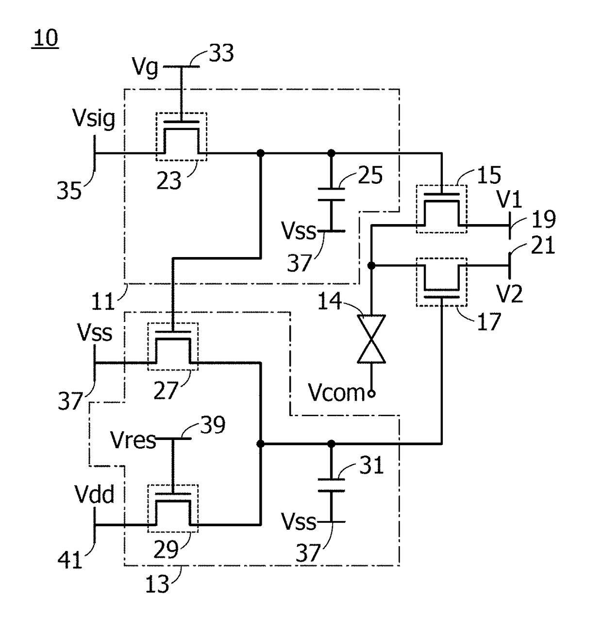
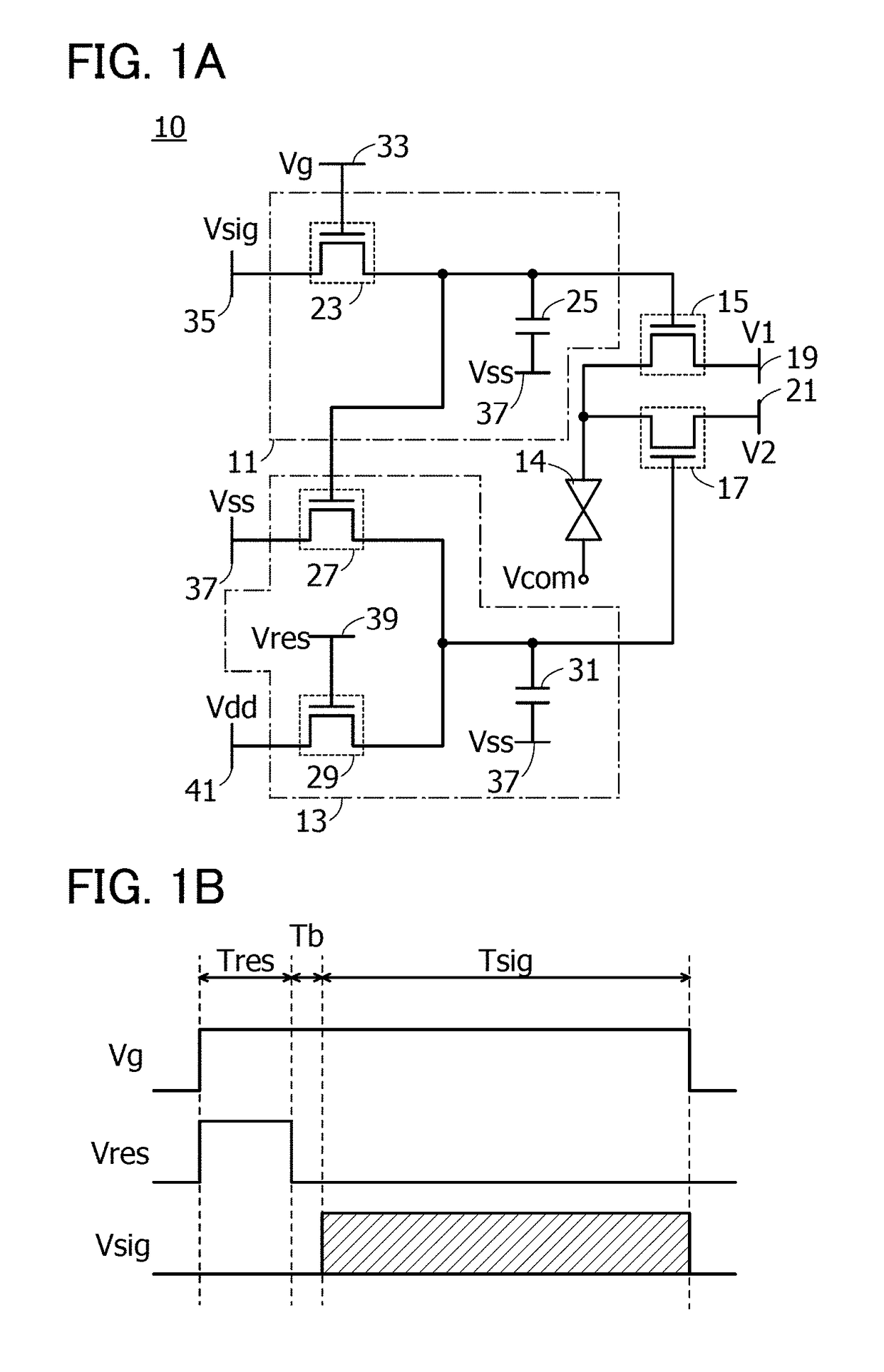
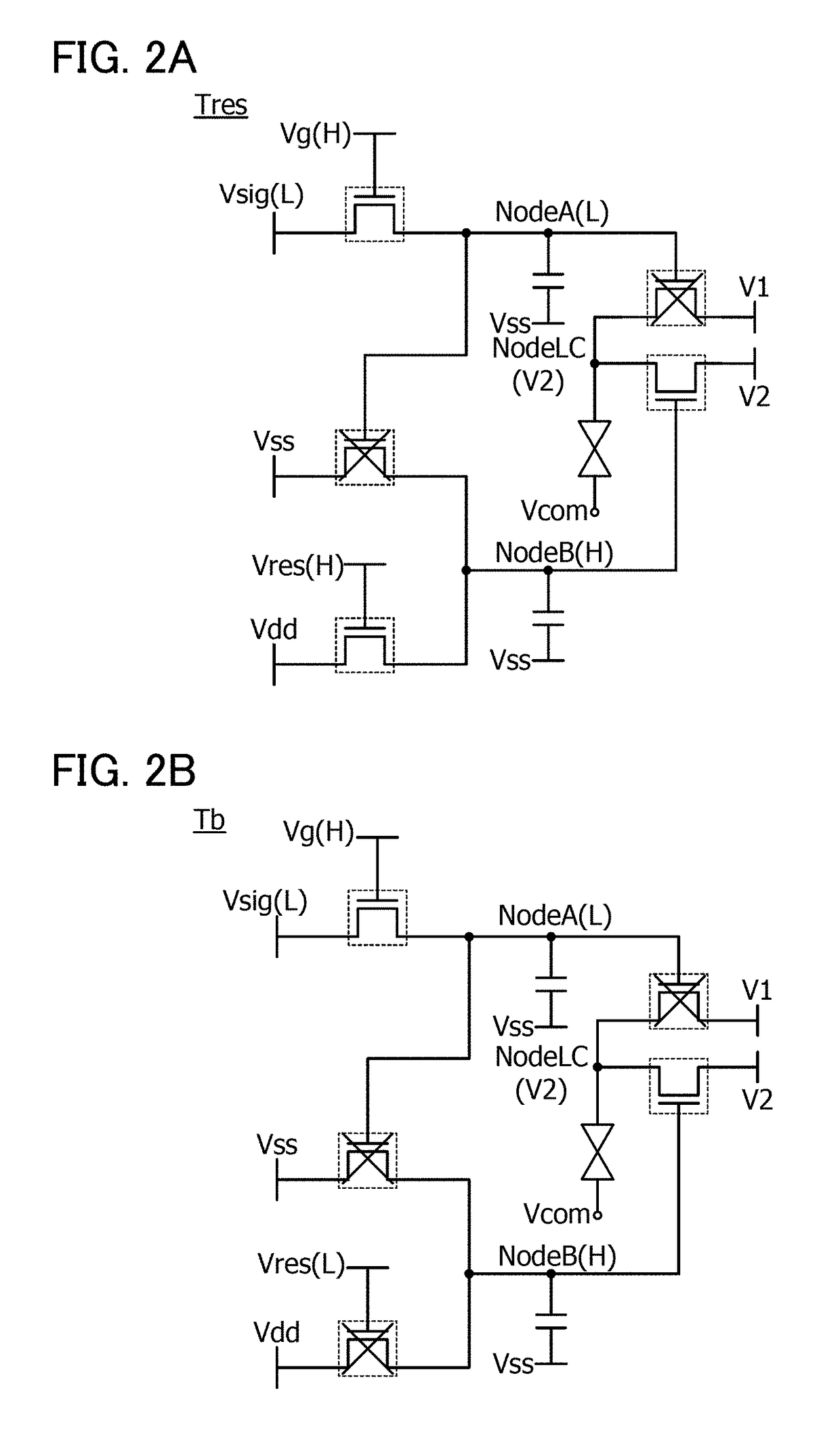
[0052]FIG. 1A is a circuit diagram of a pixel 10 included in the liquid crystal display device. FIG. 1B is a timing chart showing the operation of the pixel 10.

[0053]The pixel 10 illustrated in FIG. 1A includes a first circuit 11, a second circuit 13, a transistor 15, a transistor 17, and a liquid crystal element 14.

[0054]The first circuit 11 includes a transistor 23 and a capacitor 25.

[0055]The second circuit 13 includes a transistor 27, a transistor 29, and a capacitor 31.

[0056]The transistor 15 is turned on or off when a potential held in the first circuit 11 is supplied to its gate. The transistor 17 is turned on or ...

embodiment 2

[0114]Described in this embodiment are examples of schematic cross-sectional structures that can be used for the liquid crystal display device described above. Here, structure examples of the schematic cross section of the liquid crystal display device will be described with reference to cross-sectional views of FIGS. 9A and 9B. FIGS. 9A and 9B show examples of the cross-sectional views of a reflective liquid crystal display device.

[0115]The cross-sectional schematic view of FIG. 9A illustrates an element substrate 71, a transistor 73, a conductive layer 75 serving as a pixel electrode, a depression and projection portion 77, a liquid crystal 79, a counter substrate 81, a coloring layer 83, a light-shielding layer 85, an insulating layer 87, a conductive layer 89 serving as a counter electrode, and a polarizing plate 91.

[0116]FIG. 9B illustrates a structure different from that in the cross-sectional schematic view of FIG. 9A. In FIG. 9B, a light diffusion layer 93 is provided betwee...

embodiment 3

[0136]Described in this embodiment are examples of structures of a transistor that can be used for the liquid crystal display device described above. Here, structure examples of the cross section of the transistor will be described with reference to cross-sectional views of FIGS. 10A to 10C. FIG. 10A is a cross-sectional view of a bottom-gate transistor. FIG. 10B is a cross-sectional view of a top-gate transistor. FIG. 10C is a cross-sectional view of a dual-gate transistor.

[0137]A transistor 100A illustrated in FIG. 10A includes a conductive layer 103, an insulating layer 105, a semiconductor layer 107, a conductive layer 109A, a conductive layer 109B, an insulating layer 111, and an insulating layer 113 over a substrate 101.

[0138]Note that FIG. 10A shows a cross-sectional view of a channel-etched transistor with the bottom-gate structure; however, a channel-protective transistor may also be used. The semiconductor layer 107 may have a layered structure although FIG. 10A shows a si...


PUM

PropertyMeasurementUnit
angleaaaaaaaaaa
angleaaaaaaaaaa
angleaaaaaaaaaa

Abstract

A liquid crystal display device with a novel structure is provided. Each pixel includes a first circuit for holding a high level (or low level) potential and a second circuit for holding a low level (or high level) potential. A semiconductor layer of a transistor included in each of the first and second circuits is an oxide semiconductor layer. The second circuit is reset when being supplied with the high level potential. Whether the high level potential held in the second circuit changes is controlled by a data voltage supplied to the first circuit. The potential held in the first circuit and the potential held in the second circuit are respectively supplied to a first transistor and a second transistor.

Description

BACKGROUND OF THE INVENTION[0001]1. Field of the Invention[0002]One embodiment of the present invention relates to a display device, in particular, a liquid crystal display device.[0003]Note that one embodiment of the present invention is not limited to the above technical field. The technical field of the invention disclosed in this specification and the like relates to an object, a method, or a manufacturing method. Furthermore, the present invention relates to a process, a machine, manufacture, or a composition of matter. Specifically, examples of the technical field of one embodiment of the present invention disclosed in this specification include a semiconductor device, a display device, a light-emitting device, a power storage device, a storage device, a method for driving any of them, and a method for manufacturing any of them.[0004]2. Description of the Related Art[0005]To reduce power consumption, a reflective liquid crystal display device provided with a memory in each pix...

Claims


Application Information

Patent Timeline
Patent Type & Authority Patents(United States)
IPC IPC(8): G02F1/1362G09G3/36
CPCG02F1/13624G09G3/3659G09G2300/0852
Inventor KOYAMA, JUN
Owner SEMICON ENERGY LAB CO LTD
Why Eureka
Try Eureka