
Body tie optimization for stacked transistor amplifier

Active Publication Date: 2018-01-30
PSEMI CORP
View PDF37 Cites 32 Cited by
  • Summary
  • Abstract
  • Description
  • Claims
  • Application Information

AI Technical Summary

Benefits of technology

The present patent describes a method for improving the performance of a radio frequency (RF) amplifier by using a cascoded stack of multiple floating devices. The method involves replacing one or more of the floating devices with a body tied device, which results in an RF amplifier with improved performance. The improved performance may be achieved by using either silicon-on-insulator (SOI) technology or silicon-on-sapphire (SOS) technology. The technical effect of the patent is to provide a more efficient and effective RF amplifier for various applications.

Problems solved by technology

Floating body silicon-on-insulator (SOI) transistors are limited in operating voltage and power due to accumulated hot carriers which can increase the electrical potential of the body region of the SOI transistors.
When a floating body transistor is conducting, a corresponding floating body effect (e.g., kink) can cause abrupt reduction of output impedance of the transistor under moderate bias at various levels of drain to source voltage of the transistor, which in turn, can reduce analog gain of the transistor and increase complexity of a corresponding device modeling.
Body ties on wide (large gate width) transistors with conventional (e.g., H-gate, T-gate or other) body tie structures become less effective in suppressing device degradations due to high resistance and increased parasitic capacitance which mitigate the ability to control the floating body effects.
In particular, conventional body tied devices (e.g. H-gate, T-gate or other) are less effective in suppressing such degradations for large transistor width and the added drain to gate capacitance associated with conventional body tied devices can degrade performance in applications where such transistors are used, such as, for example, radio frequency (RF) amplifier applications.
Such degradation can be due to several factors, such as an increase in parasitic capacitance, where the parasitic capacitance can be nonlinear; a larger layout area necessary for a body tied transistor; or, in some cases, limitations of design tools whose design rules prevent design of merged transistors with body ties, therefore further increasing layout area.
For the above reasons, and in spite of benefits provided by body ties, traditional RF amplifiers using stacked SOI devices have not been fitted with body ties.
Although capacitance reduction due to the absence of body ties in SOI devices can provide some performance advantages (e.g., speed) over bulk CMOS devices, other performance parameters may suffer (e.g., voltage capability).

Method used


Image

  • Body tie optimization for stacked transistor amplifier
  • Body tie optimization for stacked transistor amplifier
  • Body tie optimization for stacked transistor amplifier

Examples


Embodiment Construction

[0029]Throughout the present description, embodiments and variations are described for the purpose of illustrating uses and implementations of the inventive concept. The illustrative description should be understood as presenting examples of the inventive concept, rather than as limiting the scope of the concept as disclosed herein.

[0030]Throughout the present description, the terms “transistor” and “device” are synonymous and can be used interchangeably.

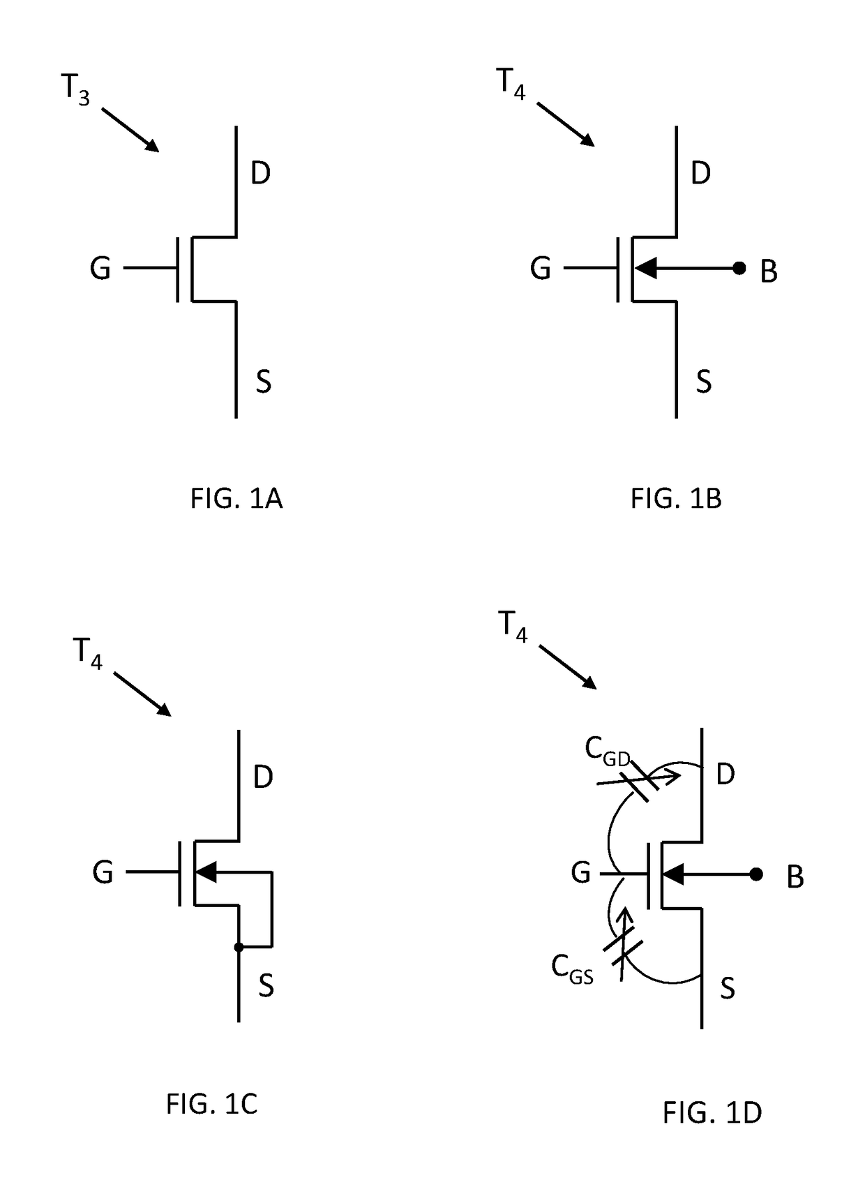
[0031]Throughout the present description, a “three-terminal” transistor is referred to as a transistor whose body is not tied to a potential and is therefore floating. A person skilled in the art would know that another expression for a three-terminal transistor is a “floating transistor”. Therefore, the expressions “three-terminal” transistor and “floating” transistor are synonymous and are used interchangeably in the present description.

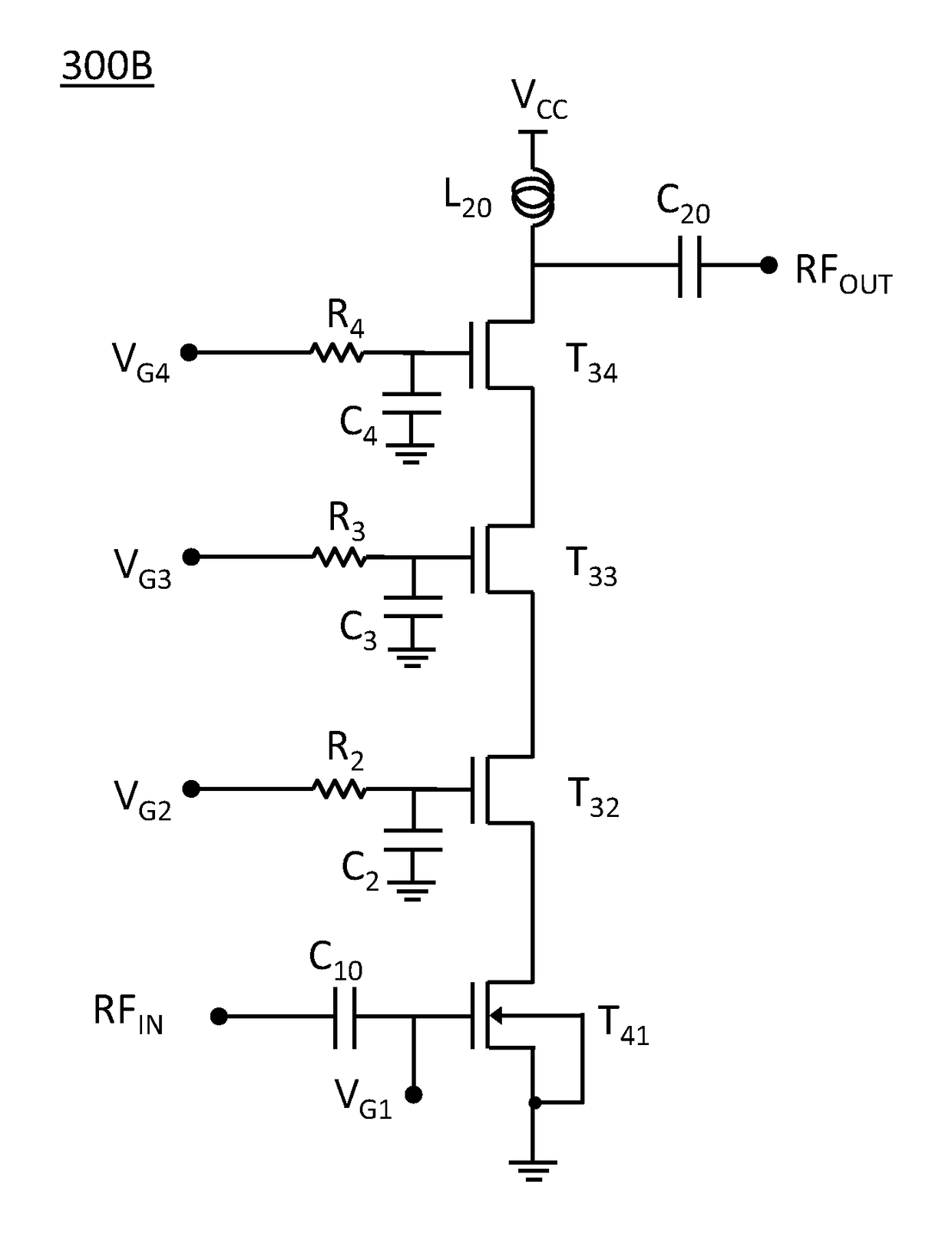
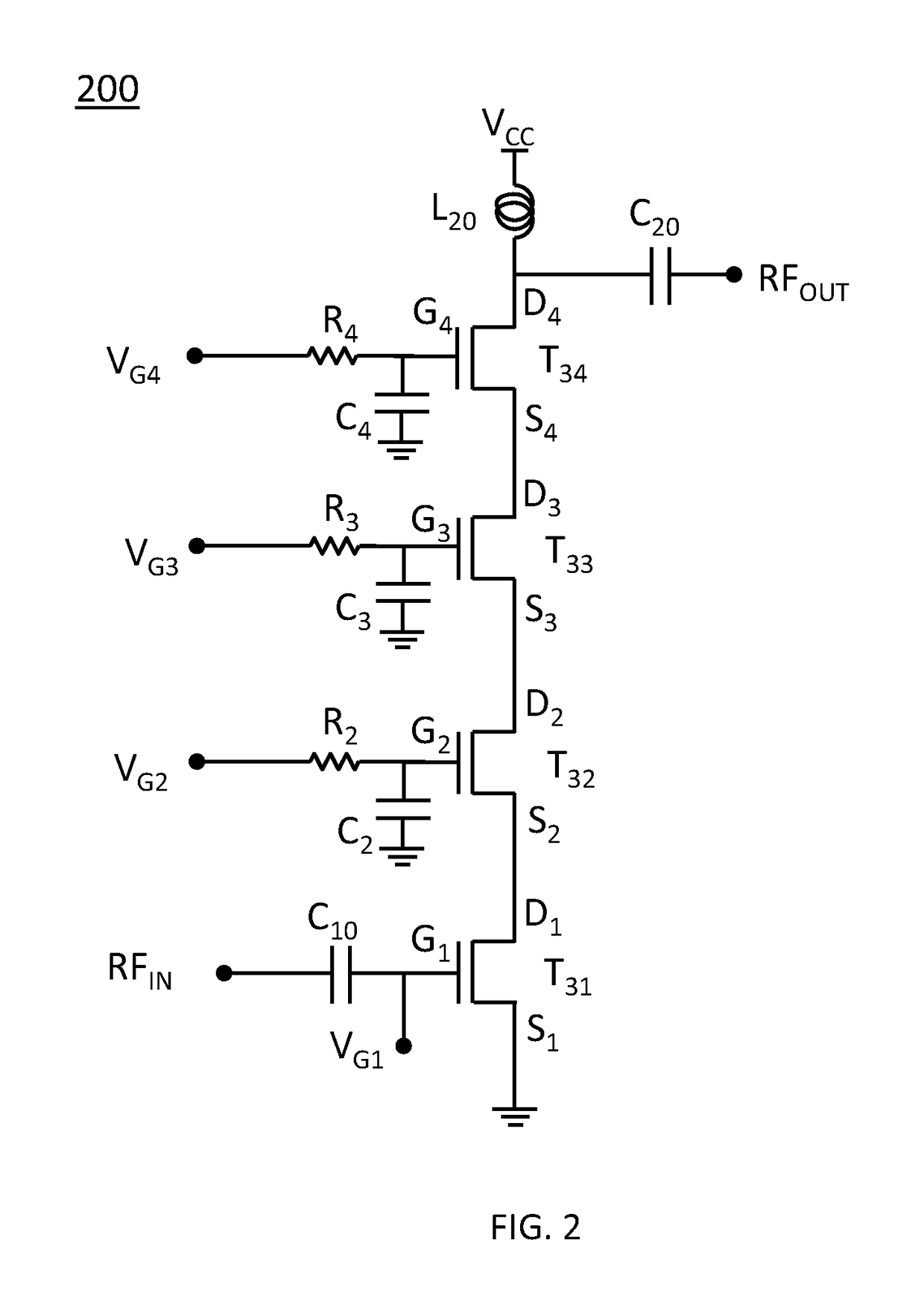
[0032]Throughout the present description, a “four-terminal” transistor is referred to as a tran...


PUM


Abstract

A transistor stack can include a combination of floating and body tied devices. Improved performance of the RF amplifier can be obtained by using a single body tied device as the input transistor of the stack, or as the output transistor of the stack, while other transistors of the stack are floating transistors. Transient response of the RF amplifier can be improved by using all body tied devices in the stack.

Description

CROSS REFERENCE TO RELATED APPLICATIONS[0001]The present application is related to U.S. application Ser. No. 15 / 268,297 entitled “Standby Voltage Condition for Fast RF Amplifier Bias Recovery” filed on Sep. 16, 2016, the disclosure of which is incorporated herein by reference in its entirety. The present application is also related to U.S. application Ser. No. 15 / 268,229 entitled “Cascode Amplifier Bias Circuits” filed on Sep. 16, 2016, the disclosure of which is incorporated herein by reference in its entirety. The present application is also related to U.S. application Ser. No. 15 / 268,275 entitled “Gate Drivers for Stacked Transistor Amplifiers” filed on Sep. 16, 2016, the disclosure of which is incorporated herein by reference in its entirety.[0002]The present application may be related to U.S. application Ser. No. 14 / 945,323, entitled “Butted Body Contact for SOI Transistor”, filed on Nov. 18, 2015, the disclosure of which is incorporated herein by reference in its entirety. The...

Claims


Application Information

Patent Timeline
IPC IPC(8): H03F1/22H01L29/08H01L27/12H01L21/84H01L29/10H01L49/02H03F1/02H03F3/193H01L27/06
CPCH03F1/0205H03F3/193H01L27/0688H01L29/1095H01L29/0847H01L27/1203H01L21/84H01L28/40H03F2200/451H03F2200/61H03F2200/297H03F2200/48H03F1/223H03F1/523H03F3/19H03F3/21H03F2200/42H03F2200/75H03F3/195H03F2200/108
Inventor WILLARD, SIMON EDWARDOLSON, CHRISRANTA, TERO TAPIO
Owner PSEMI CORP
Learn More