Stacked image sensor pixel cell with in-pixel vertical channel transfer transistor

Active Publication Date: 2018-06-05
SMARTSENS TECH (HK) CO LTD
View PDF16 Cites 8 Cited by
  • Summary
  • Abstract
  • Description
  • Claims
  • Application Information

AI Technical Summary

Benefits of technology

[0009]Another objective is to provide a pixel cell that occupies less

Problems solved by technology

However, miniaturization has come with the loss of pixel photosensitivi

Method used


Image

  • Stacked image sensor pixel cell with in-pixel vertical channel transfer transistor
  • Stacked image sensor pixel cell with in-pixel vertical channel transfer transistor
  • Stacked image sensor pixel cell with in-pixel vertical channel transfer transistor

Examples


first embodiment

[0031]In the stacked assembly illustrated in FIG. 4A and FIG. 4B the limiting die dimension is determined by the sensor chip. Assuming it is desired to retain the dimensions of the photodiode, one opportunity for further reduction to die dimension is to reduce the transfer transistor size or relocate it within the footprint of the photodiode. FIG. 5A is an exploded view diagram of a pixel cell in accordance with the invention. FIG. 5A illustrates a pixel cell layout wherein photodiode 510 and vertical channel MOSFET transfer transistor 550 are located on the semiconductor substrate of a sensor wafer or chip and pixel circuitry 511 is located on a separate substrate of a circuit semiconductor wafer or chip. FIG. 5A shows an exploded view of a sensor chip and its components positioned on its upper surface aligned at inter-chip interconnect 540 to a circuit chip with its components positioned on its underside. FIG. 5B is a cross section diagram of the pixel cell shown in FIG. 5A along ...

second embodiment

[0035]FIG. 7 is a cross section diagram of a pixel cell in accordance with the invention wherein the pixel cell is similar in structure to the pixel cell illustrated by FIG. 6 but absent insulator support structure 670. With insulator support structure 670 of FIG. 6 absent, vertical channel region 780 illustrated in FIG. 7 takes the shape of a solid cylinder or post of semiconductor material with axis perpendicular to the plane of sensor wafer substrate 725. Persons skilled in the art will recognize that post shaped structure 780 may be formed by epitaxial growth of semiconductor material within a hole formed on semiconductor substrate 725 over photodiode 710. Gate electrode 754 and thin insulator 756 may be formed as concentric toroids in the embodiment illustrated by FIG. 7 wherein vertical channel region structure 780 is shaped like a solid cylinder or post with axis perpendicular to the plane of sensor wafer substrate 625.

third embodiment

[0036]FIG. 8A is an exploded view diagram of a pixel cell in accordance with the invention. FIG. 8A illustrates a pixel cell layout wherein photodiode 810 is located on the semiconductor substrate of a sensor wafer or chip while pixel circuitry 811 and vertical channel MOSFET transfer transistor 850 are located on a separate substrate of a circuit wafer or chip. FIG. 8A shows an exploded view of a sensor chip and its components positioned on its upper surface aligned at inter-chip interconnect 840 to a circuit chip with its components positioned on its underside. FIG. 8B is a cross section diagram of the pixel cell shown in FIG. 8A along its cross section line DD′ including the overlying portion of the circuit chip. FIG. 8B illustrates the two stacked semiconductor chips shown in FIG. 8A may be electrically coupled by inter-chip interconnect 840.

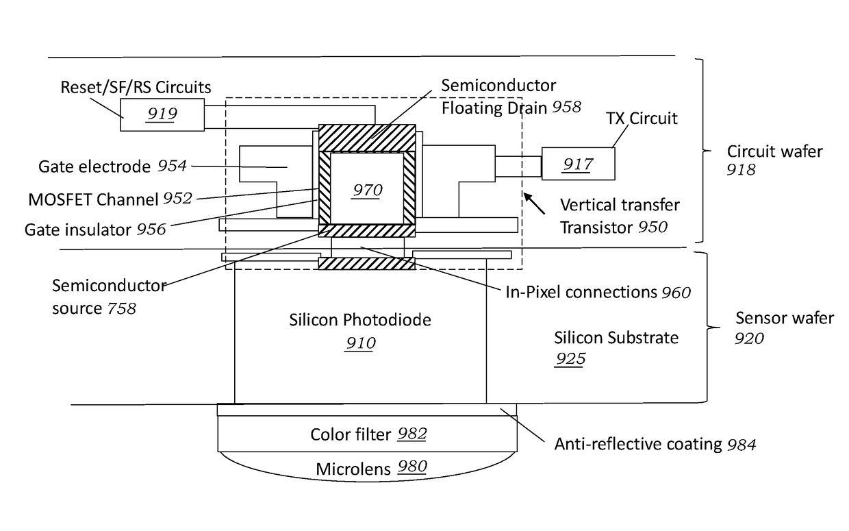
[0037]FIG. 9 is a cross section diagram of a pixel cell in accordance with a third embodiment of the invention. FIG. 9 illustrates in more ...


PUM


Abstract

A pixel cell has a photodiode, a readout circuit, and a vertical transfer transistor. The photodiode is disposed within a first substrate of a first semiconductor chip for accumulating an image charge in response to light incident upon the photodiode. The readout circuit is disposed within a second substrate of a second semiconductor chip. The vertical transfer transistor is coupled between the photodiode and the readout circuitry to transfer the image charge from the photodiode to the readout circuitry.

Description

BACKGROUND OF THE INVENTIONField of the Invention[0001]This invention relates generally to image sensors and more particularly to CMOS image sensors in a stacked chip formation. A bottom chip includes an array of light sensitive regions and structures to capture an image. A top chip includes circuit elements to extract an image from the array. The image sensor may be incorporated within a digital camera.Description of Related Art[0002]The prior art teaches a wide variety of image capture devices. A typical image capture device used in the prior art includes an image sensor and an imaging lens. The imaging lens focuses light onto the image sensor to form an image, and the image sensor converts the light into electrical signals. The electric signals are output from the image capture device to other components of a host electronic system. The image capture device and the other components of a host electronic system form an imaging system. Image sensors have become ubiquitous and may be...

Claims


Application Information

Patent Timeline
IPC IPC(8): H04N5/378H04N5/374H01L27/146
CPCH04N5/374H04N5/378H01L27/14643H01L27/14616H01L27/14689H01L27/14603H01L27/14612H01L27/14683H01L27/14638H01L27/1464
Inventor KEUNG, KO PINGXIONG, ZHIBINXU, CHENSHAO, ZEXU
Owner SMARTSENS TECH (HK) CO LTD
Why Eureka
Try Eureka