Device for reading an image having a common semiconductor layer

a semiconductor layer and image technology, applied in the direction of semiconductor devices, radio frequency controlled devices, electrical devices, etc., can solve the problems of difficult to effectively take out the carriers generated in the semiconductor by light irradiation to the outside, the compactness and lightweight of the image reading device has been further required, and the effect of improving the photoelectric conversion efficiency

Inactive Publication Date: 2006-11-14
SEMICON ENERGY LAB CO LTD
View PDF38 Cites 15 Cited by
  • Summary
  • Abstract
  • Description
  • Claims
  • Application Information

AI Technical Summary

Benefits of technology

[0011]In order to overcome the above disadvantagedisadvantages of the prior art, an object of this invention is to provide a device for reading an image (an image reading device) which has a compact structure, high photoresponsibility and highly-effective photosensitivity and is capable of reading out an image with high precision and high gradation.
[0015]The photoelectric conversion device and the thin film transistor are formed of the same semiconductor film, and formation of impurity semiconductor regions of the photoelectric conversion device and that of the thin film transistor are carried out at the same time, e.g. by ion implantation, thereby implementing simplification of a manufacturing process and reduction of a manufacturing cost.
[0019]Further, the semiconductor film may be composed of semi-amorphous or semi-crystal semiconductor. In this case, the semiconductor film has a long diffusion length which can not be obtained by amorphous semiconductor, and a large absorption coefficient which is not obtained by monocrystal or polycrystal semiconductor. Therefore, the semiconductor film can be thinned and the photoelectric conversion device having a long diffusion length can be manufactured.
[0021]In the photoelectric conversion device thus constructed, those carriers which are generated in a photoelectric converting area between the P-type and N-type diffusion regions can be effectively outputted to the outside because of the long diffusion length of the semiconductor layers. In addition, since the P-type and N-type impurity regions are formed in a direction of depth (in a laminating direction) of the same semiconductor film from the light-irradiating surface of the semiconductor film, the intensity of the irradiated light is constant in the direction of the electric field between the P-type and N-type impurity regions, so that photoelectric conversion efficiency is improved.

Problems solved by technology

However, a more compact and lightweight of image reading device has been further required for these types.
As a result, it is difficult to effectively generate electrons / holes in the conventional photoelectric conversion device and output them to the outside.
Further, the photoelectric conversion device using amorphous semiconductor has a disadvantage that it is difficult to effectively take out carriers generated in the semiconductor by light irradiation to the outside because the semiconductor material has a short diffusion length.
As described above, miniaturization, high photoresponsibility and effectivity of photosensitivity have been insufficient to the conventional image reading device, and thus a further development has been required for the conventional image reading device.

Method used


Image

  • Device for reading an image having a common semiconductor layer
  • Device for reading an image having a common semiconductor layer
  • Device for reading an image having a common semiconductor layer

Examples


first embodiment

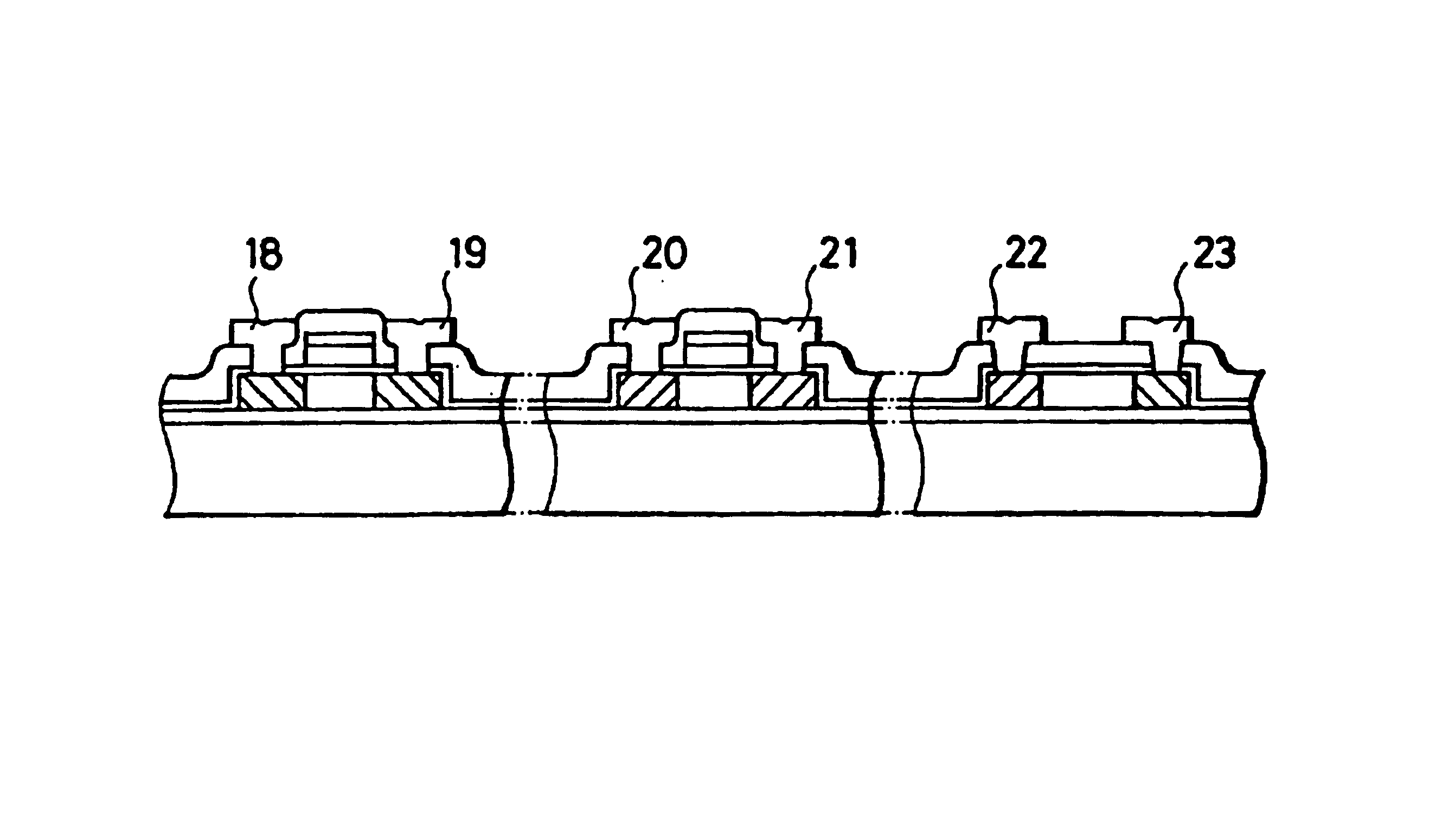
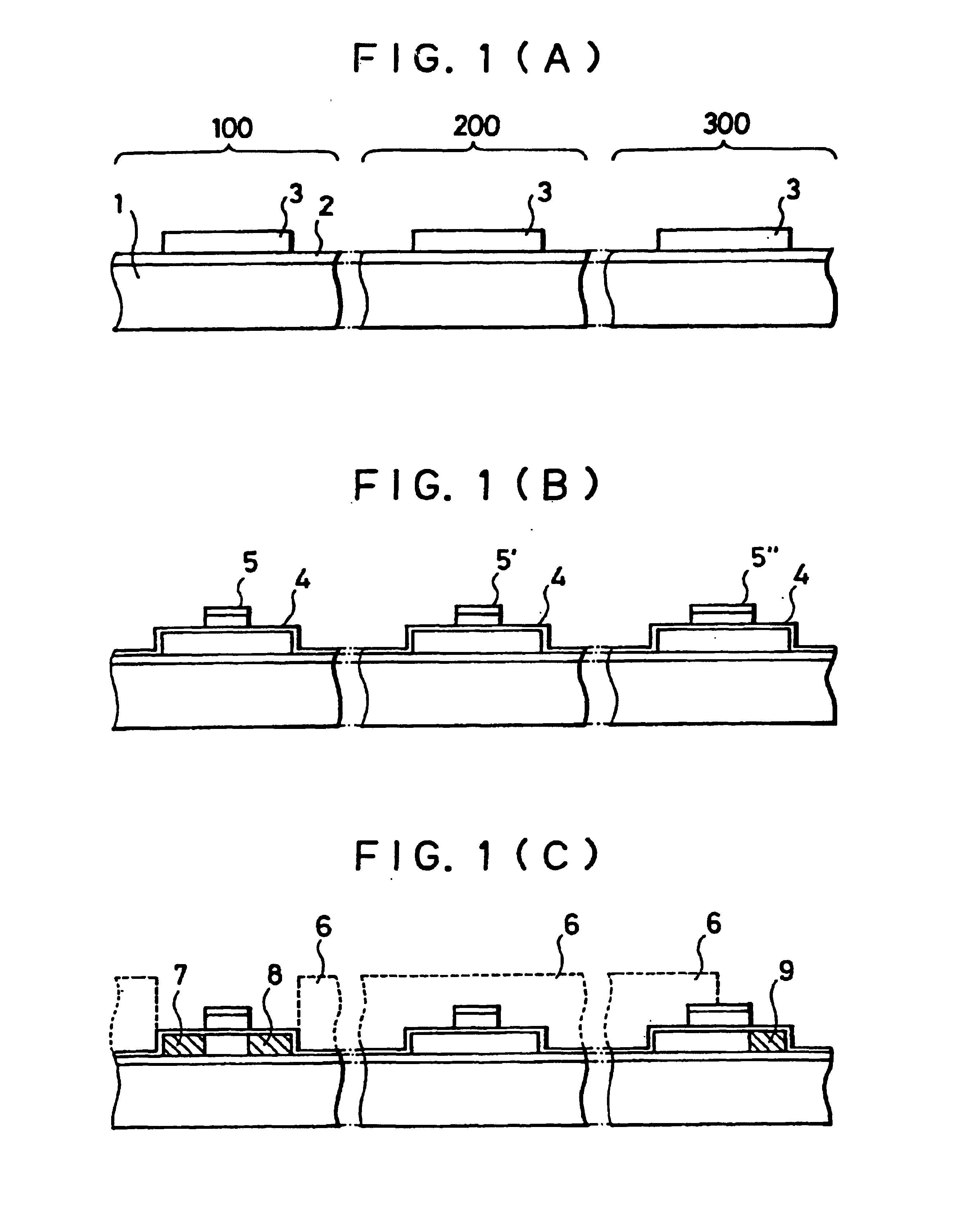
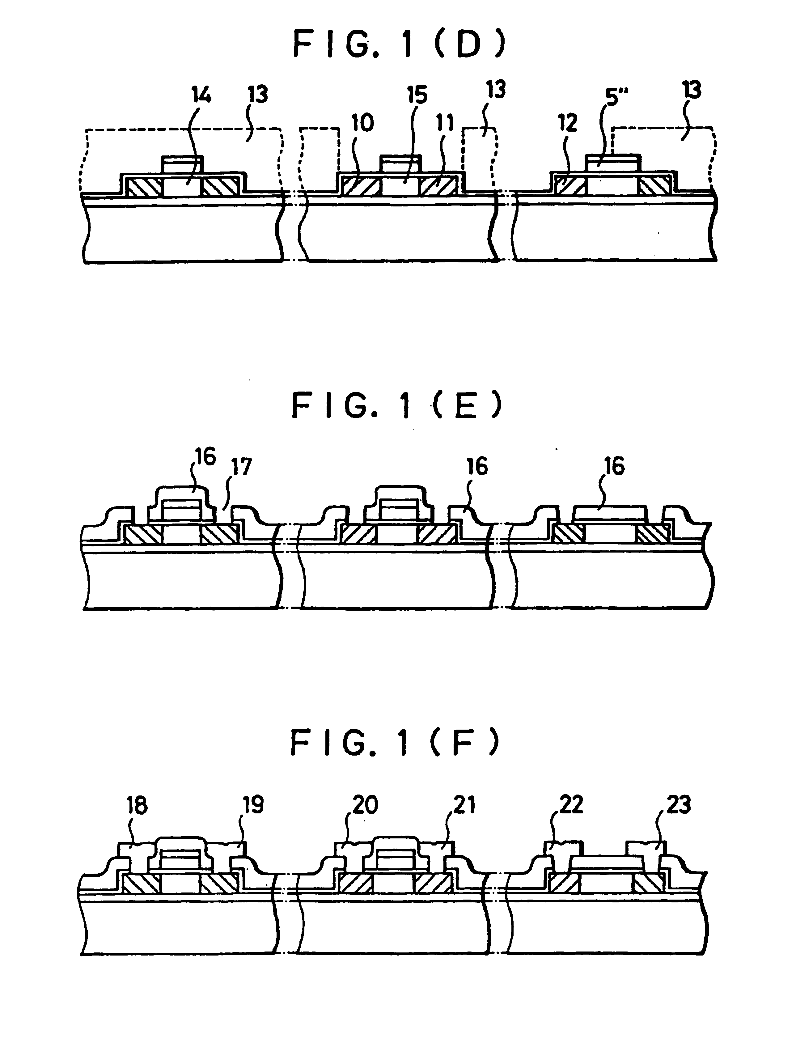
[0035]FIGS. 1(A) to 1(F) are longitudinal-sectional views showing a manufacturing process for an image reading device according to this invention, and in particular a manufacturing process for a photoelectric conversion device portion and P-type and N-type TFT portions.

[0036]In FIG. 1(A), a substrate 1 comprises a conductive or insulating substrate. For example, pottery, ceramic or glass material is used as a substrate in this embodiment. The reason for utilization of these materials resides in that these materials have low cost, high mechanical strength and heat-resistance for a film forming process.

[0037]In FIG. 1, reference numerals 100, 200 and 300 represent a P-channel TFT (P-type thin film transistor) portion, an N-channel TFT (N-type thin film transistor) portion and a photoelectric conversion device portion, respectively. The substrate 1 comprises glass material such as AN glass, Pyrex glass or the like which has a heat-resistance against a thermal process at a temperature o...

second embodiment

[0067]FIG. 2 shows another embodiment of the photoelectric conversion device portion of the image reading device, which has substantially the same structure as that of the first embodiment, except that an amorphous silicon semiconductor film 24 of 3000 Å in thickness is further formed on a light-irradiating surface side of the semiconductor film 3. The other film-forming processes are identical to those of the first embodiment.

[0068]The amorphous silicon semiconductor film 24 has a larger absorption coefficient than that of the semiconductor film 3. Accordingly, upon light-irradiation, a large amount of carriers are produced in the amorphous silicon semiconductor film 24, and then drift through the semiconductor film 3 and are outputted through the positive and negative electrodes to the outside.

[0069]At the same time, carriers are also produced in the semiconductor film 3. The photosensitivity of the semiconductor film 3 is dependent on the wavelength of the irradiated light. There...

third embodiment

[0072]The image reading device of this third embodiment has substantially the same construction as the first embodiment, except for the following point.

[0073]Only the N-type TFT includes the same semiconductor film as used for the photoelectric conversion device, and is formed simultaneously with the formation of the N-type impurity region of the photoelectric conversion device 300. At the time when the P-type impurity region is formed in the photoelectric conversion device portion 100, the TFT portion is masked by a photoresist, and thus no P-type impurity is doped. In this embodiment, unlike the complementary type of TFT, it is not necessary to coincide Vth between the P-type TFT and the N-type TFT. Accordingly, a permissible range for the manufacturing process is broadened.

[0074]In the embodiments as described above, the light is irradiated from an opposite side to the substrate. However, the light-irradiating direction is not limited to the above direction, and the light may be ...


PUM


Abstract

A device for reading an image (an image reading device) according to this invention comprises therein at least one photoelectric conversion semiconductor device provided on a substrate and at least one thin film transistor circuit element provided on the substrate wherein said photoelectric conversion semiconductor device and said thin film transistor circuit element comprise semiconductor regions obtained from one semiconductor film provided on said substrate. The device for reading an image is produced by a process comprising the steps of: depositing a semiconductor material on a substrate; forming a photoelectric conversion semiconductor device on said substrate, a semiconductor region of said photoelectric conversion semiconductor device being made of said semiconductor material; and forming a thin film transistor on said substrate, a semiconductor region of said thin film transistor being made of said semiconductor material, wherein said thin film transistor constitutes an electric circuit required to read an image.

Description

BACKGROUND OF THE INVENTION[0001]1. Field of the Invention[0002]This invention relates to a device for reading an image (an image reading device), and more particularly to a device for reading an image (an image reading device) having photoelectric conversion devices arranged in a transverse direction to an original, which is usable for a facsimile machine, an image reader, a digital copying machine and the like.[0003]2. Description of the Prior Art[0004]As this type of image reading apparatus as described above have been conventionally known three types of image reading devices such as a non-contact type, a close contact type and an entirely-close contact type. Recently, in association with requirement for a compact and lightweight type of facsimile machine, image reader, digital copying machine or the like, the image reading apparatus itself is required to be compact and lightweight. This requirement causes the close contact and entirely-close contact types to be mainly propagated...

Claims


Application Information

Patent Timeline
Patent Type & Authority Patents(United States)
IPC IPC(8): H01L27/14H01L21/8238H01L27/092H01L27/12H01L27/146H01L29/78H01L29/786H01L31/10
CPCH01L27/1203H01L27/14665
Inventor YAMAZAKI, SHUNPEI
Owner SEMICON ENERGY LAB CO LTD
Why Eureka
Try Eureka