Method for improving organic electro-luminescence device lifetime
A technology of device life and luminescence, which is applied in the direction of electroluminescence light source, electric light source, electrical components, etc., can solve the problems that affect the life of the device, interface instability, corrosion, etc., and achieve the effect of improving the life of the device
- Summary
- Abstract
- Description
- Claims
- Application Information
AI Technical Summary
Problems solved by technology
Method used
Image
Examples
Embodiment Construction
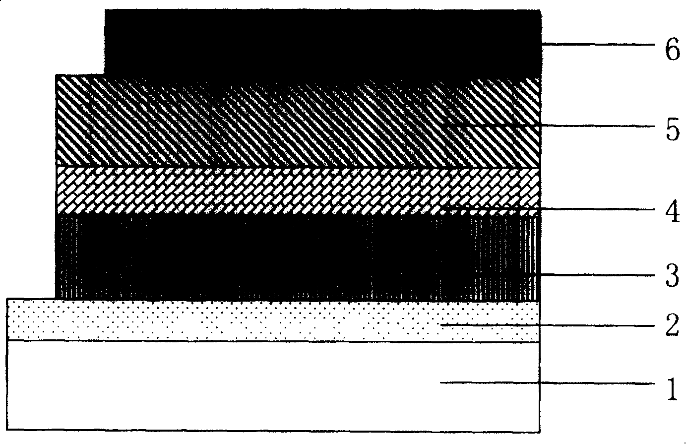
[0028] Firstly, a conductive polymer hole injection layer with a thickness of about 40nm is formed by spin-coating on the carefully cleaned indium tin oxide (ITO) transparent conductive anode (1) substrate (2) Polyethylenedioxythiophene-polyphenylene Ethylene sulfonic acid (PEDOT:PSS) film is then placed in the vacuum chamber of the reactive ion etching machine, and the oxygen in the vacuum chamber is ionized by radio frequency discharge method to generate oxygen plasma to properly surface the surface of the conductive polymer hole injection layer. Treatment, oxygen plasma treatment power density is about 50mW / cm 2 , the air pressure is about 2.0Pa, the gas flow is about 40sccm, and the treatment time is 5 minutes and 8 minutes respectively, which can be formed on the surface of the conductive polymer hole injection layer (2) to improve its effective interaction with the hole transport layer (3). Nanoscale microstructures of contact and interface properties (e.g. Figure 3 sh...
PUM
 Abstract
Description
Claims
Application Information


