High-absorption wide-band pixel for bolometer arrays
A microradiometer and pixel technology, applied in the field of thermal imaging, can solve the problems of sensitivity, high absorption, and high manufacturing cost, and achieve the effects of reducing manufacturing cost, increasing temperature range, and wide infrared spectrum bandwidth
- Summary
- Abstract
- Description
- Claims
- Application Information
AI Technical Summary
Problems solved by technology
Method used
Image
Examples
Embodiment Construction
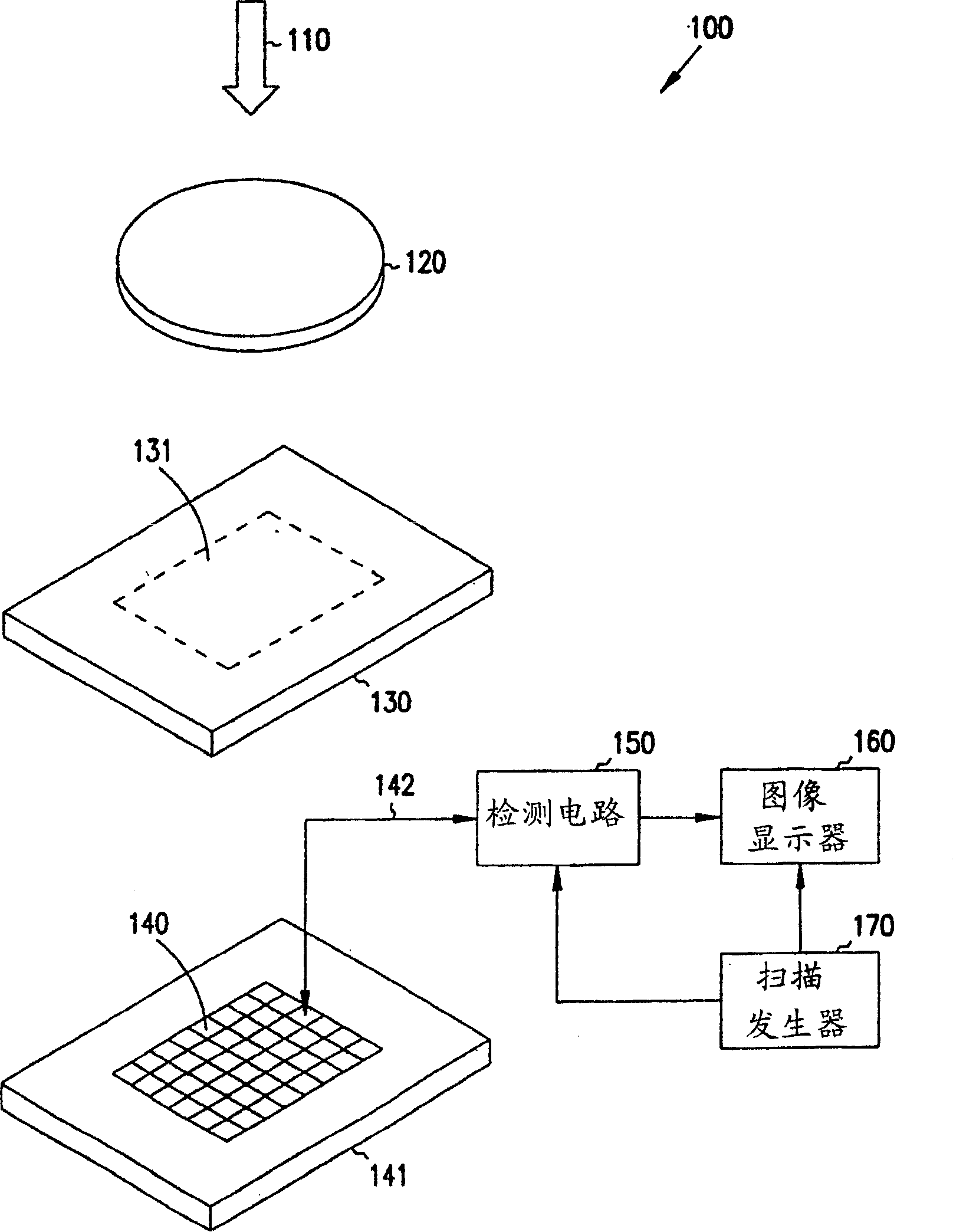
[0011] figure 1 is a stylized view of a typical infrared imaging detector 100 having pixels constructed in accordance with the present invention. Arrow 110 represents infrared radiation generated by a thermal body and emitted to infrared imaging optics 120 designed by conventional techniques. The component 130 has a window region 131 which is transparent for the infrared wavelengths for transmitting the radiation 110 . In many applications, it is desirable to seal and evacuate the assembly 130 in order to increase sensitivity and pixel-to-pixel isolation, and to reduce contamination and aging.
[0012] The rectangular bolometer array 140 in the assembly 130 is fabricated on a substrate of silicon or similar material with suitable electrical and micromachining properties. A typical array has a side length of 5-15mm. In many applications, such as night vision imagers, array 140 operates at ambient temperatures, such as in the range of about -40°C to +100°C. However, it is al...
PUM
 Abstract
Description
Claims
Application Information


