High-absorption wide-band pixel for bolometer arrays

A microradiometer and pixel technology, applied in the field of thermal imaging, can solve the problems of high absorption, sensitivity, and high manufacturing cost, and achieve the effects of wide infrared spectrum bandwidth, reduced manufacturing cost, and increased temperature range

Inactive Publication Date: 2004-04-28
HONEYWELL INT INC
View PDF0 Cites 1 Cited by
  • Summary
  • Abstract
  • Description
  • Claims
  • Application Information

AI Technical Summary

Problems solved by technology

Wide bandwidths are difficult to achieve, and the array is sensitive to a large number of interacting factors in the structure and materials in each individual pixel
When the array is not cooled to cryogenic temperatures, noise can overwhelm the useful signal
Good sensitivity to small temperature differences requires high absorpt

Method used


Image

  • High-absorption wide-band pixel for bolometer arrays
  • High-absorption wide-band pixel for bolometer arrays
  • High-absorption wide-band pixel for bolometer arrays

Examples


Embodiment Construction

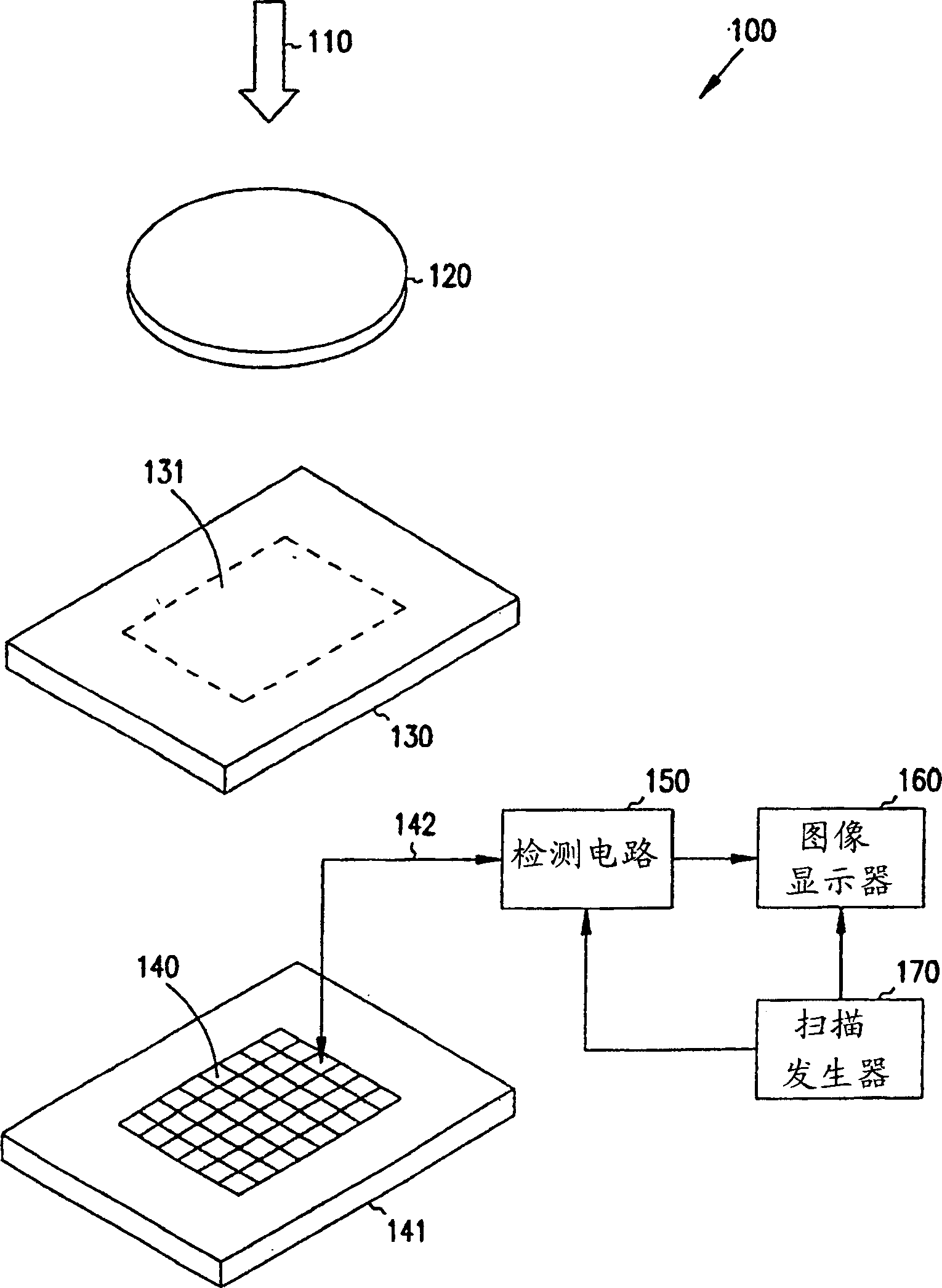
[0011] figure 1 is a stylized view of a typical infrared imaging detector 100 having pixels constructed in accordance with the present invention. Arrow 110 represents infrared radiation generated by a thermal body and emitted to infrared imaging optics 120 designed by conventional techniques. The component 130 has a window region 131 which is transparent for the infrared wavelengths for transmitting the radiation 110 . In many applications, it is desirable to seal and evacuate the assembly 130 in order to increase sensitivity and pixel-to-pixel isolation, and to reduce contamination and aging.

[0012] The rectangular bolometer array 140 in the assembly 130 is fabricated on a substrate of silicon or similar material with suitable electrical and micromachining properties. A typical array has a side length of 5-15mm. In many applications, such as night vision imagers, array 140 operates at ambient temperatures, such as in the range of about -40°C to +100°C. However, it is al...


PUM

PropertyMeasurementUnit
Thicknessaaaaaaaaaa
Thicknessaaaaaaaaaa

Abstract

A microbolometer array has pixels with a thin platform of silicon dioxide having a metal absorber layer, and having a resonant gap with a substrate reflector. The pixel resistor of vanadium oxide has low total resistance with metal contacts on opposite edges.

Description

technical field [0001] The present invention relates to thermal imaging, and more particularly to improved pixels or cells for bolometer arrays. Background technique [0002] Night vision and related applications are achieved by receiving infrared radiation emitted by a thermal body by a detector array whose electrical output signals are converted into a visual image. Individual detectors called cells, elements or pixels must be very small. Also they should be sensitive to a very broad infrared spectrum, have minimal noise at ambient temperature, operate with high sensitivity and be cheap to manufacture. [0003] Arrays of uncooled bolometers on semiconductor substrates offer a promising method for room temperature infrared imaging. Such arrays have disadvantages in several different ways. Wide bandwidths are difficult to achieve, and the array is sensitive to a large number of interacting factors in the structure and materials in each individual pixel. When the array is...

Claims


Application Information

Patent Timeline
IPC IPC(8): G01J5/02G01J1/02G01J5/20G01J5/48H01L27/14H04N5/33
CPCG01J5/20G01J5/00
Inventor B·E·科尔
Owner HONEYWELL INT INC
Why Eureka
Try Eureka