
Advanced lighting system for micro light carving method

一种照明系统、照明光学系统的技术,应用在微光刻曝光设备、图纹面的照相制版工艺、光学等方向,能够解决曝光光学部件可变相干性等问题,达到简单光学部件的效果

Inactive Publication Date: 2008-07-30
ASML HLDG NV
View PDF8 Cites 2 Cited by
  • Summary
  • Abstract
  • Description
  • Claims
  • Application Information

AI Technical Summary

Problems solved by technology

However, a particular problem arises in the field of microlithography where the different features that need to be formed on semiconductor substrates require partially exposed optics with variable partial coherence

Method used


Image

  • Advanced lighting system for micro light carving method
  • Advanced lighting system for micro light carving method
  • Advanced lighting system for micro light carving method

Examples


Embodiment Construction

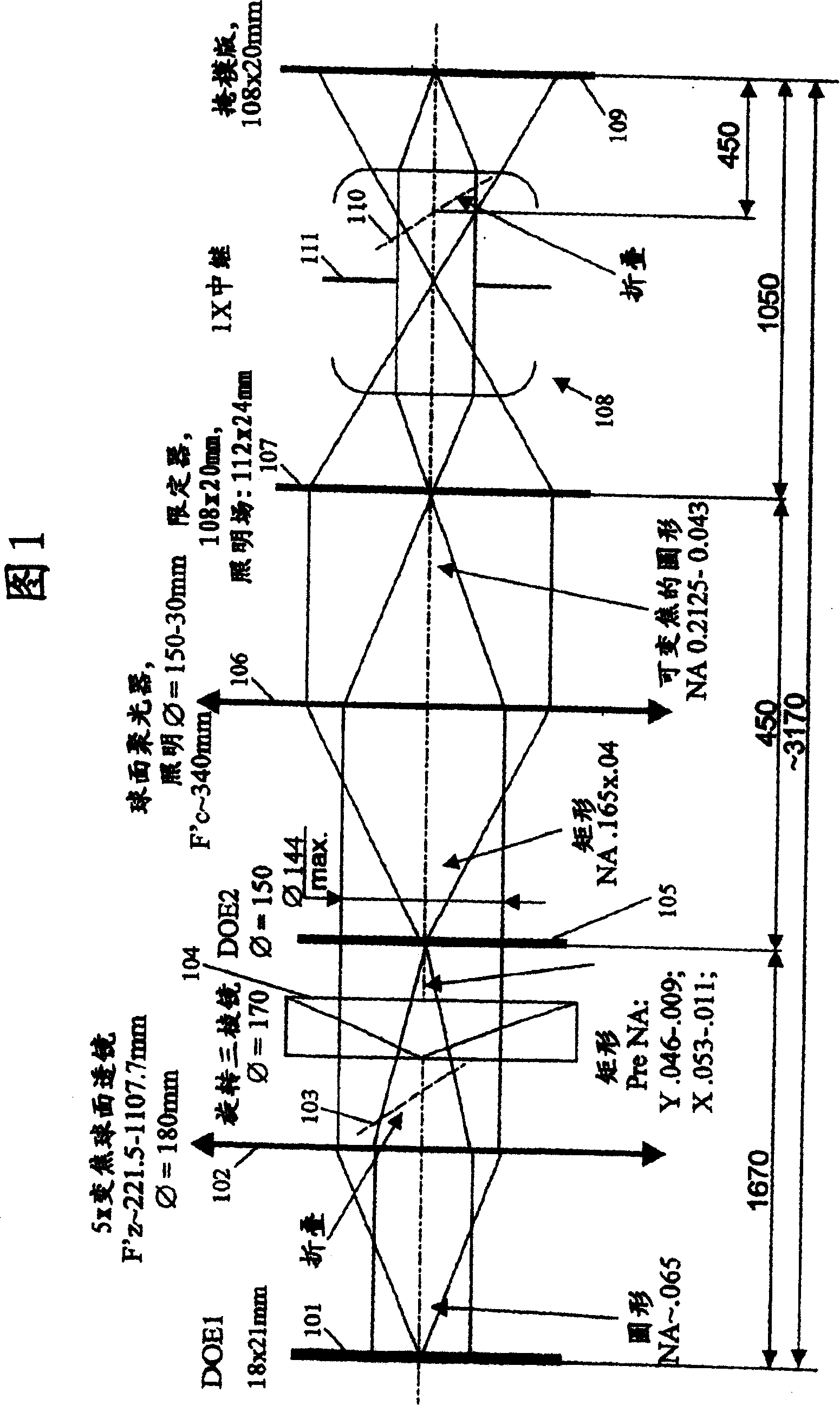
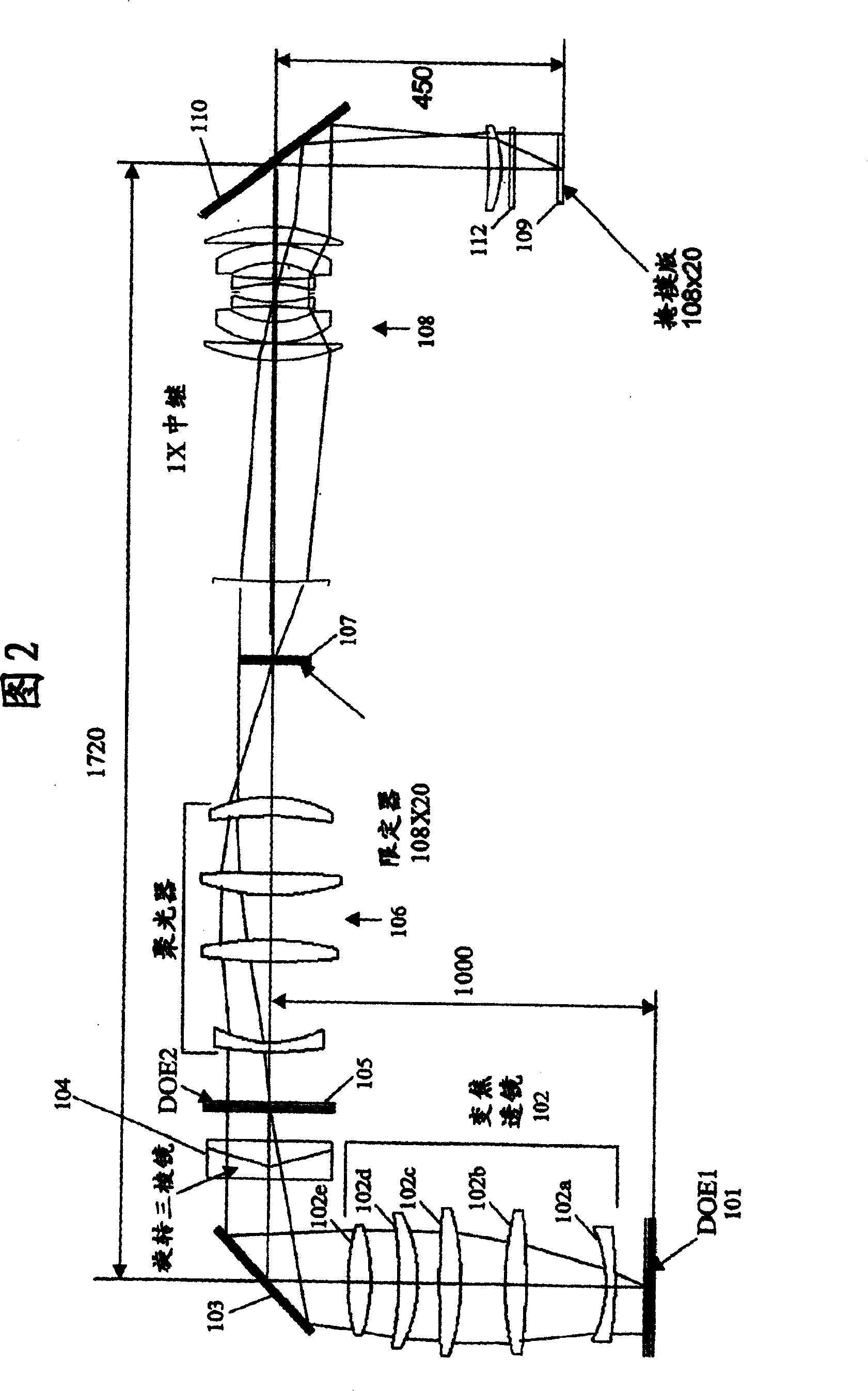
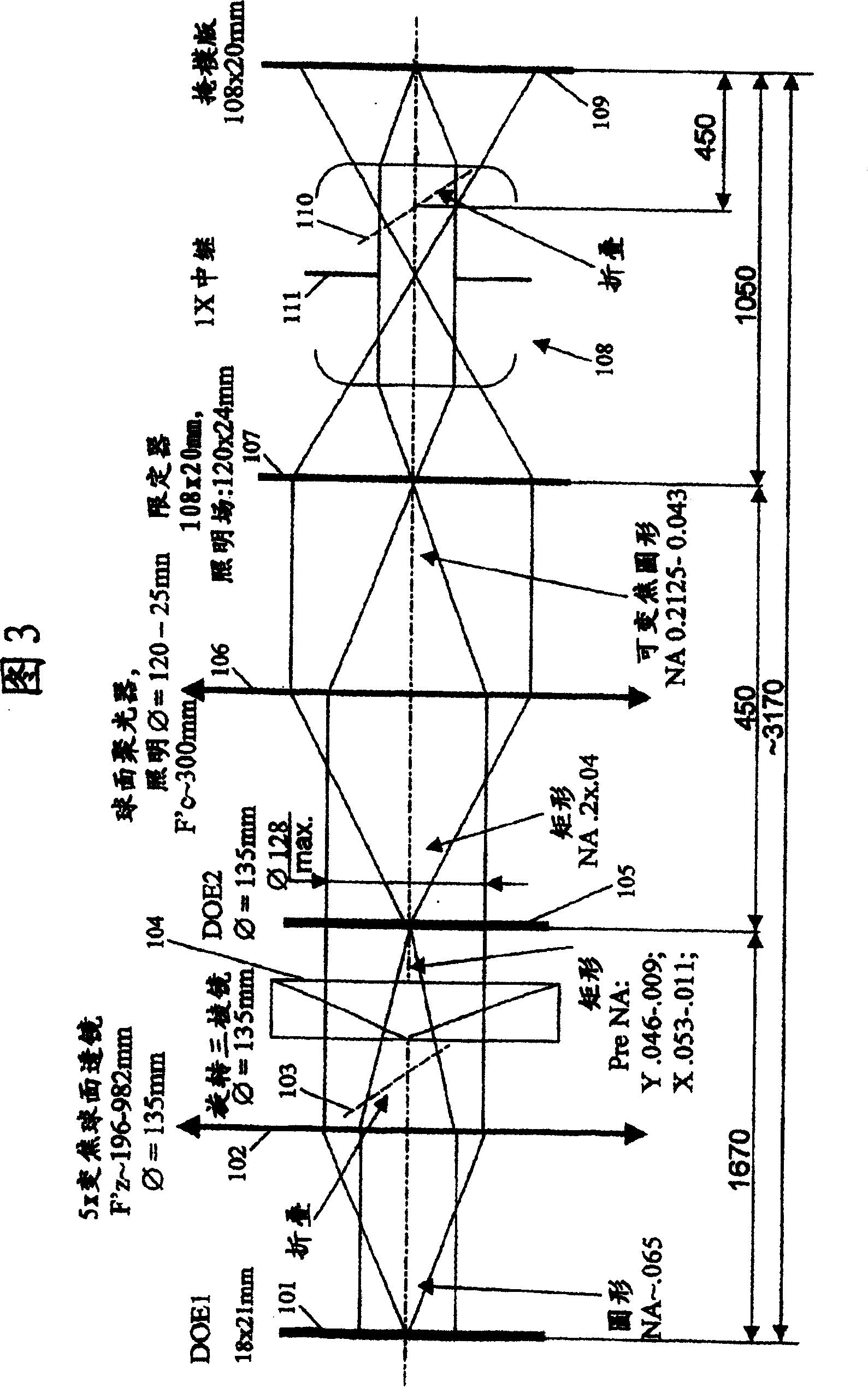
[0028] Reference will now be made in detail to the preferred embodiments of the present invention, examples of which are illustrated in the accompanying drawings.

[0029] In recent years, the photolithography methods used to fabricate semiconductor devices have gradually moved to shorter wavelengths as device features shrink in size. With feature sizes shrinking to the sub-micron, and sub-0.1 micron range, semiconductor manufacturers have had to change to using ultraviolet light, and in some cases soft X-ray lithography (or deep UV). For example, excimer lasers, which emit light in the 248, 193, and 157 nm range, are increasingly used in semiconductor device fabrication. The illumination source in a modern microlithographic apparatus, as noted above, is usually a visible laser, an excimer laser, or possibly a soft X-ray source. (The terms "light" and "illumination" will be used interchangeably herein to refer to any electromagnetic radiation applied to the photoresist). The...


PUM

PropertyMeasurementUnit
lengthaaaaaaaaaa
lengthaaaaaaaaaa
lengthaaaaaaaaaa

Abstract

A method and system allow for changing (continuously or variably) both a field height and pupil of a beam that illuminates an object field. In one example, the object field can have a pattern generator (e.g., one or more reticles, spatial light modulators, or the like) positioned therein. The system and method for changing both the field height and the pupil can include a field defining element, a pupil defining element, and first and second zoom systems. The field defining element (FDE) can generate a field height of an illumination beam. The first zoom system can allow for changing of the field height of the illumination beam. The pupil defining element (PDE) can generate a pupil of the illumination beam. The second zoom system can allow for changing of the pupil of the illumination beam.

Description

technical field [0001] This invention relates to microlithography and, more particularly, to illumination systems having high numerical apertures for microlithography equipment. Background technique [0002] Photolithography (also known as microlithography) is used to fabricate semiconductor devices. Photolithography uses electromagnetic radiation, such as ultraviolet (UV), deep UV, or visible light, to produce detailed patterns in semiconductor device designs. Many kinds of semiconductor devices, such as diodes, transistors, and integrated circuits, can be fabricated using photolithographic techniques. In semiconductor fabrication, photolithographic techniques such as etching are performed with exposure systems or equipment. An exposure system typically includes an illumination system, a reticle (also known as a mask) containing a circuit pattern, a projection system, and a wafer alignment stage for aligning a photoresist-coated semiconductor wafer. The illumination syst...

Claims


Application Information

Patent Timeline
Patent Type & Authority Patents(China)
IPC IPC(8): G03F7/20G02B27/42G02B3/00H01L21/027G02B19/00G02B13/18G02B13/22G02B13/26G02B15/167
CPCG03F7/70183G03F7/70091G03F7/70158G03F7/20
Inventor 马克·奥斯考特斯凯莱福·雷日科夫斯高特·考斯坦詹姆斯·察考印尼斯沃特·奥格斯特茵
Owner ASML HLDG NV
Learn More