
Method of forming bank, method of forming film pattern, device, and electronic apparatus

A cofferdam and pattern technology, applied in the direction of instruments, circuits, electrical components, etc., can solve the problems of poor contact holes and inability to form contact holes well

Inactive Publication Date: 2009-04-29
SEIKO EPSON CORP
View PDF5 Cites 0 Cited by
  • Summary
  • Abstract
  • Description
  • Claims
  • Application Information

AI Technical Summary

Problems solved by technology

[0008] Especially in the case where the formed bank is used to form the upper layer wiring pattern after the second layer, and a contact hole (contact hole) is formed between the upper layer wiring pattern and the conductive part of the lower layer and conduction, if the upper layer wiring pattern If the above-mentioned residue remains in the formation area, the contact hole cannot be formed satisfactorily, which may result in a defective contact hole

Method used


Image

  • Method of forming bank, method of forming film pattern, device, and electronic apparatus
  • Method of forming bank, method of forming film pattern, device, and electronic apparatus
  • Method of forming bank, method of forming film pattern, device, and electronic apparatus

Examples


no. 1 Embodiment approach

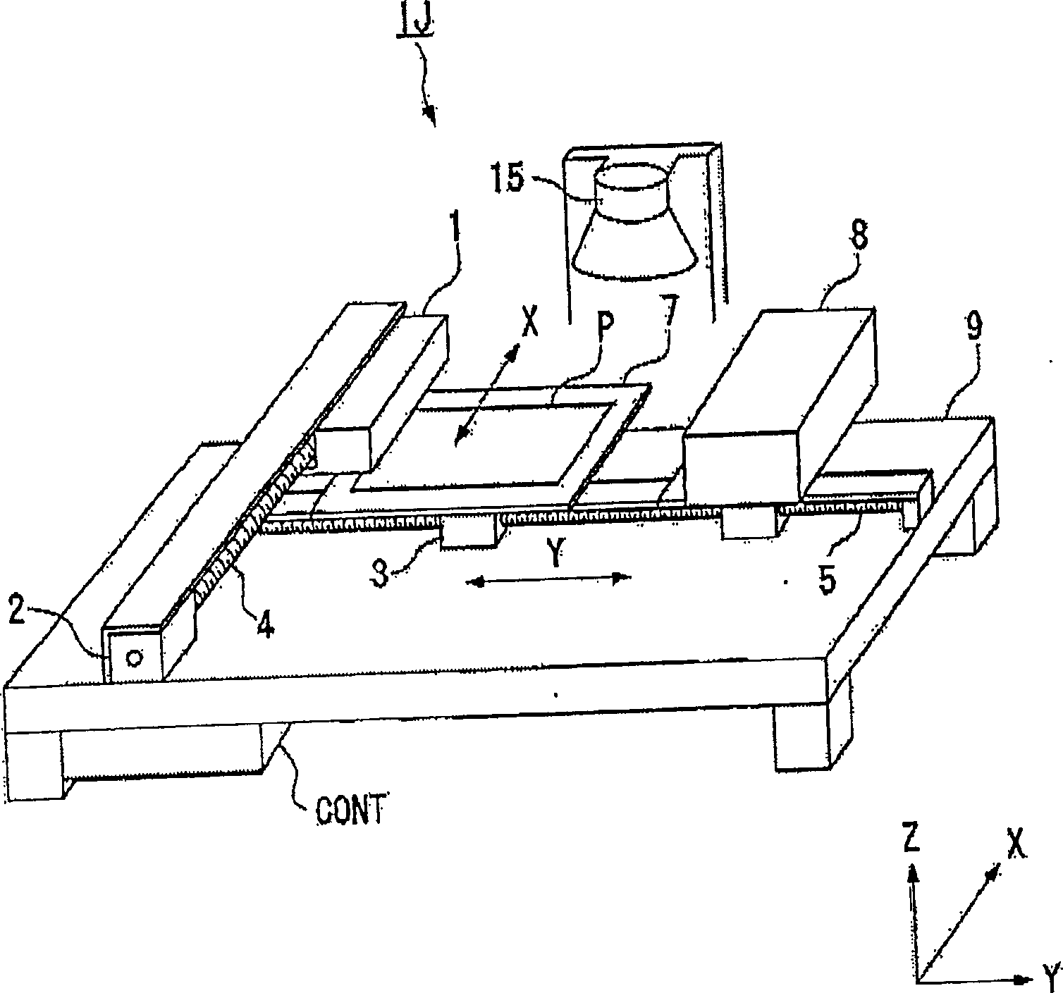
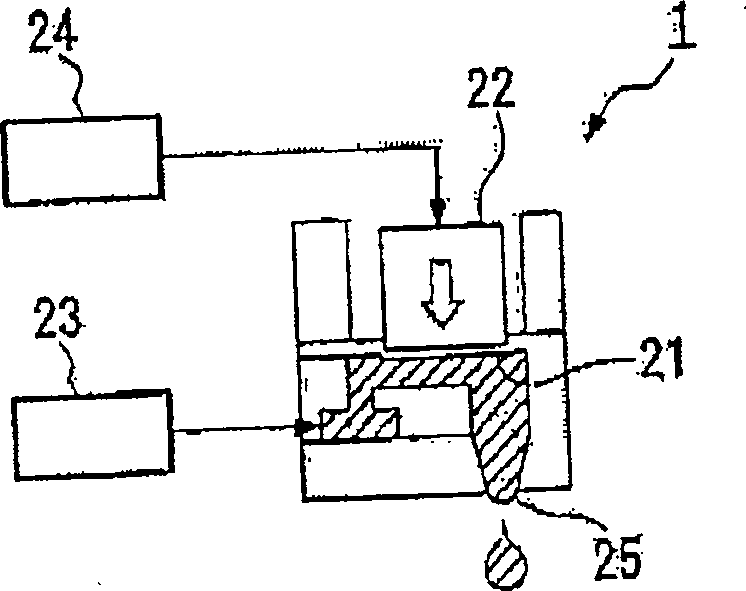
[0057] First, in the film pattern forming method of the present invention, the ink (functional liquid) for wiring patterns (film patterns) containing conductive fine particles is ejected in droplet form from the nozzles of the droplet ejection head by the droplet discharge method, and the corresponding wiring pattern An embodiment in which a wiring pattern (film pattern) is formed in a concave portion of a bank formed on a substrate, that is, in a region partitioned by the bank will be described.

[0058] Here, the wiring pattern ink (functional liquid) is constituted by a dispersion liquid in which conductive fine particles are dispersed in a dispersant. In this embodiment, in addition to metal fine particles containing at least one of gold, silver, copper, aluminum, chromium, manganese, molybdenum, titanium, palladium, tungsten, and nickel as the conductive fine particles, their oxidized particles are also used. substances and conductive polymers or superconductor particles,...

no. 2 Embodiment approach

[0129] Next, another embodiment in the case where the method for forming a film pattern of the present invention is used for a method for forming a wiring pattern (film pattern) will be described.

[0130] The difference between this embodiment and the previous embodiments is that Figure 5 The ultraviolet irradiation treatment (ultraviolet irradiation process) shown in (c) and Figure 5 The exposure processing (exposure process) shown in (d) is performed simultaneously.

[0131] That is, in this embodiment, if Figure 5 As shown in (b), the lyophobic treatment is carried out in the cofferdam membrane 31, and after the lyophobic treatment layer 37 is formed on its surface, as Figure 9 As shown, the ultraviolet irradiation treatment and the exposure treatment were simultaneously performed using one mask M. For such processing, for example, the processing device has an exposure light source for irradiating light such as G-line (254nm), H-line (365nm), and I-line (405nm), and...

no. 3 Embodiment approach

[0137] Next, another embodiment of the method for forming a film pattern of the present invention will be described. In this embodiment, circuit wiring (wiring pattern) is further formed on the wiring pattern (film pattern) formed in the previous first or second embodiment. In addition, the droplet discharge method, the droplet discharge device, and the manufactured semiconductor device, etc., used in this embodiment are the same as the droplet discharge method, droplet discharge device, and semiconductor device in the first embodiment. Basically the same.

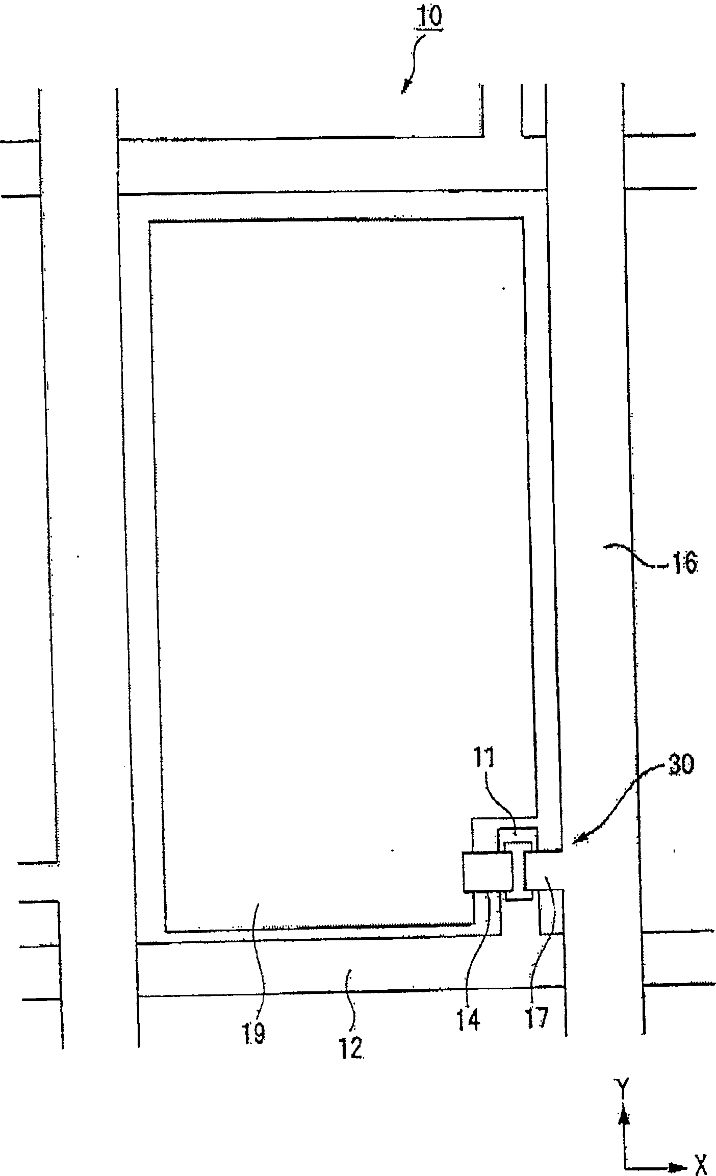
[0138] In this embodiment, first as Figure 10 As shown in (a), on the gate wiring 12 (gate electrode 11) as a wiring pattern formed in the first or second embodiment, a gate insulating film (insulating film 28) as a semiconductor layer is formed by plasma CVD. Active layer 63 and bonding layer 64 are successively formed. The silicon nitride film as the insulating film 28 , the amorphous silicon film as the active layer...


PUM

PropertyMeasurementUnit
particle diameteraaaaaaaaaa
surface tensionaaaaaaaaaa

Abstract

A method of forming a bank that partitions a region for forming a film pattern made of a functional liquid, includes: forming a bank film made of a photo resist by applying a photo resist liquid onto a substrate and drying the photo resist liquid; performing a lyophobic treatment for the bank film by using a lyophobic treatment gas and plasma; reducing a lyophobic property by selectively applying ultraviolet rays to the bank film after the lyophobic treatment with a mask; selectively exposing the bank film after the lyophobic treatment to light with the mask; developing and patterning the bank film after reducing the lyophobic property and exposing the bank film to light so as to form the bank; wherein the lyophobic property is reduced and the bank film is exposed to light continuously or at the same time with the same mask.

Description

technical field [0001] The present invention relates to a method of forming a bank, a method of forming a film pattern, a semiconductor device, an electro-optical device, and an electronic device. Background technique [0002] A conventionally known semiconductor device is a semiconductor device in which a circuit wiring including a thin film (film pattern) made of a conductor, a thin film such as an insulating film covering the circuit wiring, and a thin film made of a semiconductor are stacked on a substrate. As described in Patent Document 1, a method for efficiently forming a thin film in such a semiconductor device is known, in which droplets of a functional liquid containing a thin film material or the like as a dispersoid are ejected from a droplet nozzle, and the dropped functional liquid is dried and dried. Droplet discharge method (inkjet method) that removes the dispersant and forms a thin film. [0003] In the case of forming a thin film as a film pattern by the...

Claims


Application Information

Patent Timeline
Patent Type & Authority Patents(China)
IPC IPC(8): H01L21/288H01L21/336H01L21/02G03F7/00
Inventor 守屋克之平井利充
Owner SEIKO EPSON CORP
Learn More