Check patentability & draft patents in minutes with Patsnap Eureka AI!

Plasma etching method

A plasma and etching technology, applied in the field of shallow trench isolation, can solve the problems of increased leakage current and increased power consumption, and achieve the effect of suppressing leakage current and saving power

Inactive Publication Date: 2009-07-15
TOKYO ELECTRON LTD
View PDF5 Cites 0 Cited by
  • Summary
  • Abstract
  • Description
  • Claims
  • Application Information

AI Technical Summary

Problems solved by technology

As a result, there is a problem that leakage current between the gate electrode and the active region increases due to the shoulder, which causes an increase in power consumption.

Method used


Image

  • Plasma etching method
  • Plasma etching method
  • Plasma etching method

Examples


Embodiment Construction

[0044] Hereinafter, preferred embodiments of the present invention will be described with reference to the drawings.

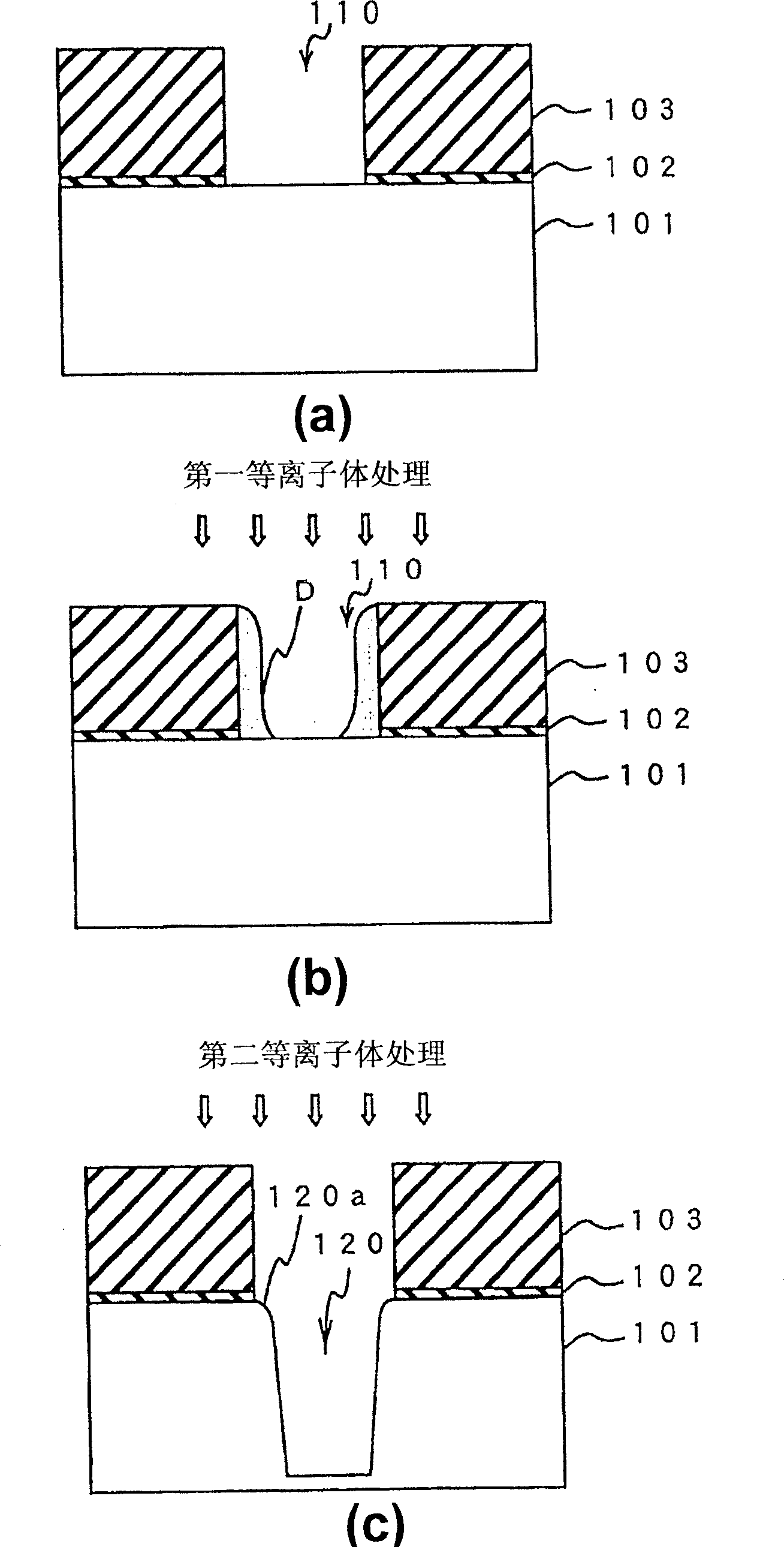
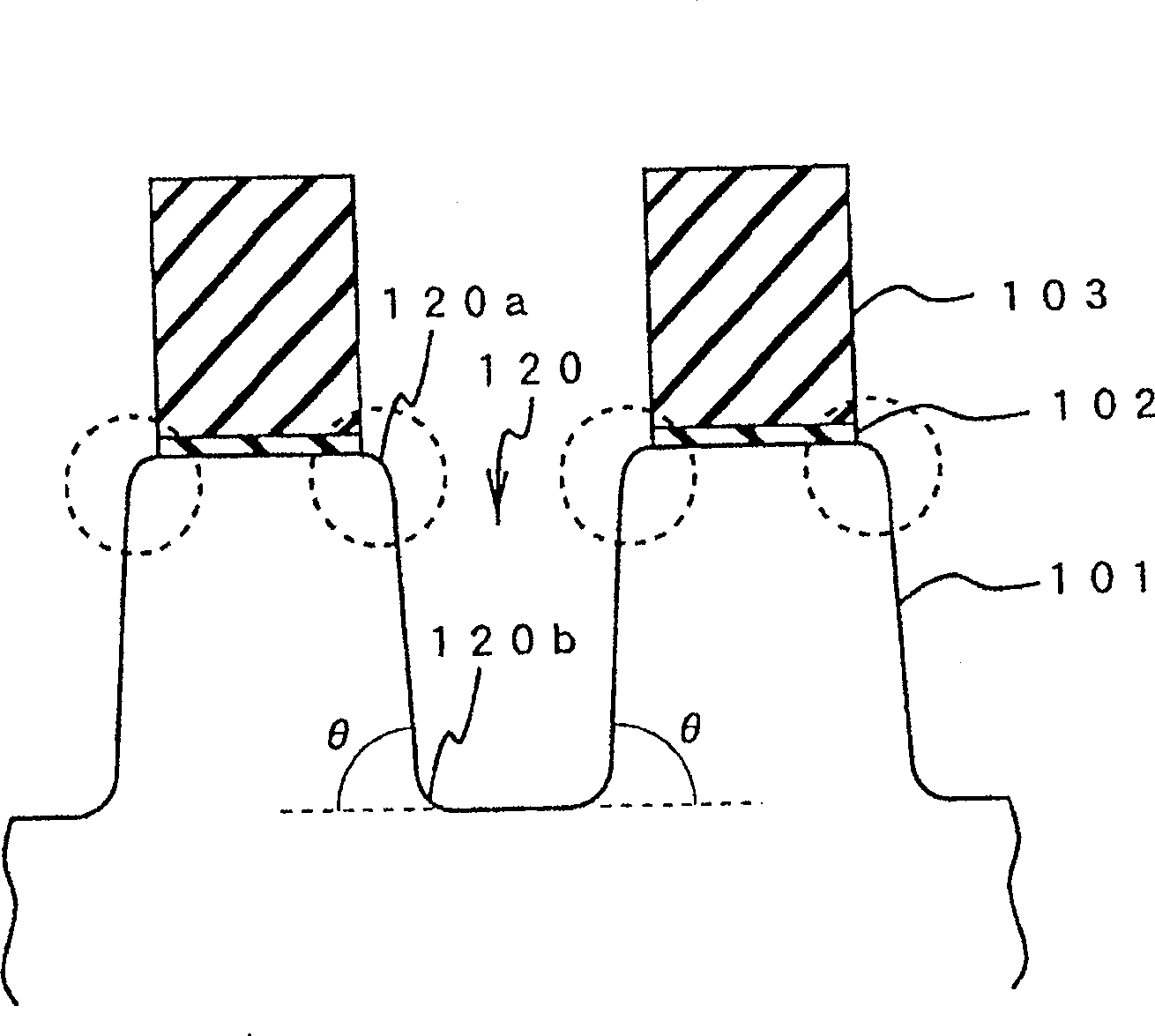
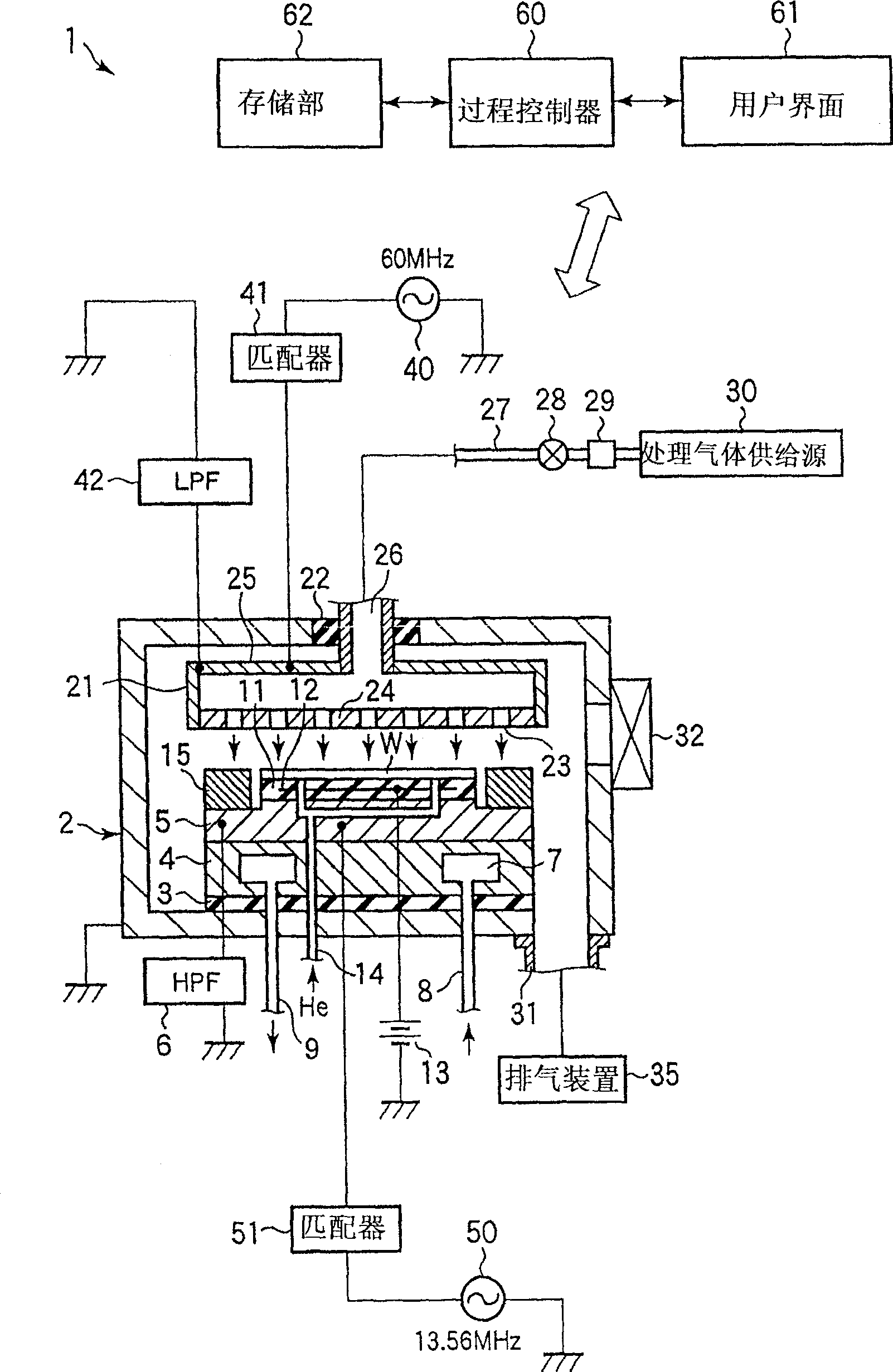
[0045] figure 1 It is a schematic diagram showing a main part of a longitudinal section of a semiconductor wafer (hereinafter simply referred to as "wafer") W in a silicon trench etching process such as enlarged STI for explaining one embodiment of the present invention. like figure 1 As shown in (a), on the silicon substrate 101 constituting the wafer W, for example SiO 2 etc. silicon oxide film 102, and on it, for example, form Si 3 N 4 and so on silicon nitride film 103 . The silicon nitride film 103 functions as a hard mask.

[0046] The silicon nitride film 103 and the silicon oxide film 102 are patterned into a predetermined shape to form a mask layer. figure 1 In (a), the groove part 110 which is the opening which comprises a pattern is shown in figure. In addition, the patterning of the silicon nitride film 103 and the silicon oxide film 102 is ...


PUM


Abstract

The present invention provides an etching method for forming a groove on a silicon substrate with high precision, and quickly performing processing while maintaining a rounded shoulder of the groove. In the first plasma treatment, a gas containing hydrofluorocarbons such as CHF3, CH2F2, CH3F is used to form a deposit (D) on at least a side wall of the trench portion (110). In the next second plasma treatment, the silicon substrate (101) is plasma etched using an etching gas to form a trench (120). The deposition (D) formed by the first plasma treatment acts as a protective film, and the etching rate of the silicon substrate (101) decreases near the sidewall of the trench (110), so the shoulder of the trench (120) formed The portion (120a) is formed to have a circular curved shape.

Description

technical field [0001] The present invention relates to a plasma etching method, and in particular relates to a method applicable to forming, for example, trenches in shallow trench isolation (Shallow Trench Isolation; STI), which is an element isolation technology in the manufacturing process of semiconductor devices. Plasma etching method. Background technique [0002] STI is known as a technique for electrically separating elements formed on a silicon substrate. In STI, the silicon nitride film is used as a mask to etch the silicon to form a trench, and the SiO 2 After the insulating film is buried therein, it is planarized by chemical mechanical polishing (CMP; Chemical Mechanical Polishing) using the mask (silicon nitride film) as a stopper. [0003] However, in recent years, in response to demands for higher integration and higher speed of LSIs, the design rules of semiconductor elements constituting LSIs have become more and more fine-grained, and at the same time, ...

Claims


Application Information

Patent Timeline
Patent Type & Authority Patents(China)
IPC IPC(8): H01L21/3065H01L21/76
Inventor 清水昭贵冈广实
Owner TOKYO ELECTRON LTD
Features
  • R&D
  • Intellectual Property
  • Life Sciences
  • Materials
  • Tech Scout
  • Unparalleled Data Quality
  • Higher Quality Content
  • 60% Fewer Hallucinations
Learn More