System for displaying image and method for laser annealing for cryogenic polycrystalline silicon

A technology of low-temperature polysilicon and polysilicon, which is applied in the manufacture of transistors, electrical components, semiconductors/solid-state devices, etc. It can solve the problems of dissimilar current characteristics of thin film transistors, difficult maintenance, high cost, etc., to improve electron mobility and increase melting time , the effect of saving the cost of use

Inactive Publication Date: 2009-10-07
TPO DISPLAY
View PDF3 Cites 0 Cited by
  • Summary
  • Abstract
  • Description
  • Claims
  • Application Information

AI Technical Summary

Problems solved by technology

[0005] When in the excimer laser annealing process, the excimer laser EL is irradiated on the amorphous silicon thin film layer 15, because the irradiation energy of the excimer laser EL is evenly distributed on the amorphous silicon thin film layer 15, so the amorphous silicon thin film layer 15 is gradually made It is in a semi-molten state, and part of the unmelted silicon will first be used as a seed crystal for recrystallization, and then grow into crystal grains, so finally a polysilicon film layer 15 with uniform distribution and the same particle size but smaller crystal grain size is formed. The crystal particles of the polysilicon thin film layer 15 are relatively small, so not only the current characteristics of the thin film transistors are not similar, but also the electron mobility of the thin film transistors cannot be improved; in addition, when the excimer laser EL irradiates the amorphous silicon thin film layer 15, Because the gate electrode 13 below the amorphous silicon film layer 15 is metal, it has a heat conduction effect, so that the crystallized particles of the silicon film near the gate electrode 13 are smaller, but the polysilicon region near the gate electrode 13 is used as a thin film transistor. When the channel area is used, if the polysilicon crystal particles in the channel area are too small, it will not only reduce the electron mobility of the thin film transistor, but also affect the performance of the LTPS TFT display
[0006] In addition, due to the high cost of using excimer laser EL, the service life of excimer laser EL is short and difficult to maintain; on the other hand, the grain size formed by the excimer laser tempering process is too small, and the size uniformity It is not easy to control and has a serious impact on the electron mobility of thin film transistors

Method used


Image

  • System for displaying image and method for laser annealing for cryogenic polycrystalline silicon
  • System for displaying image and method for laser annealing for cryogenic polycrystalline silicon
  • System for displaying image and method for laser annealing for cryogenic polycrystalline silicon

Examples


Embodiment Construction

[0063] In order to further explain the technical means and effects that the present invention adopts to achieve the intended purpose of the invention, the system for displaying images and the laser annealing method for low-temperature polysilicon proposed according to the present invention will be specifically described below in conjunction with the accompanying drawings and preferred embodiments. Embodiments, structures, methods, steps, features and effects thereof are described in detail below.

[0064] A system for displaying images and a laser annealing method for low temperature polysilicon according to preferred embodiments of the present invention will be described below with reference to related drawings, wherein the same elements will be described with the same reference symbols.

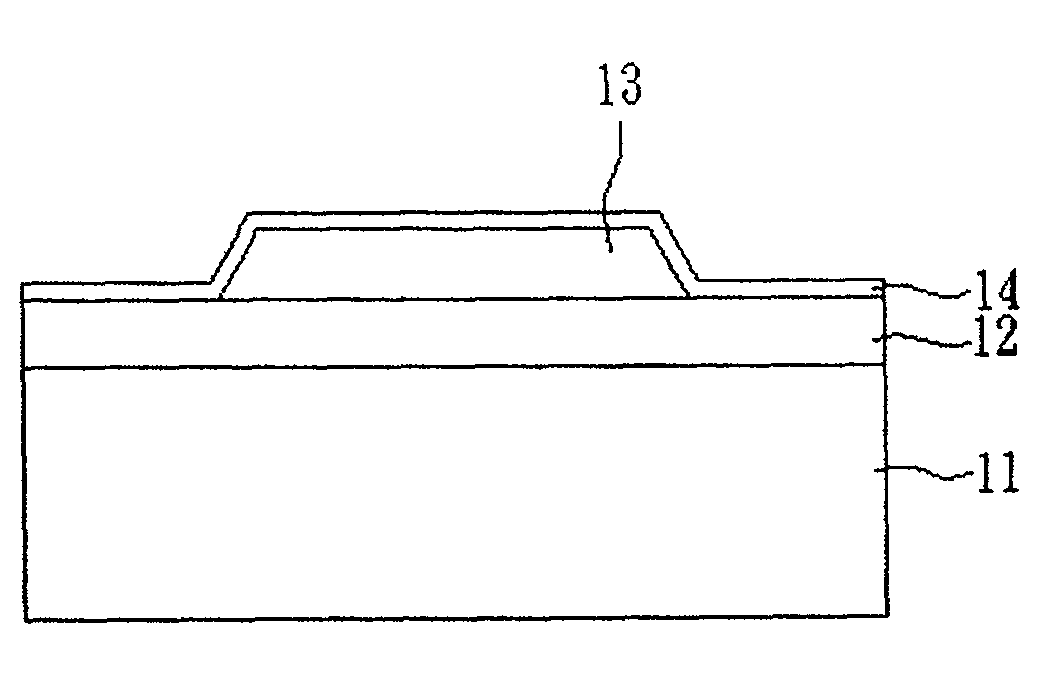
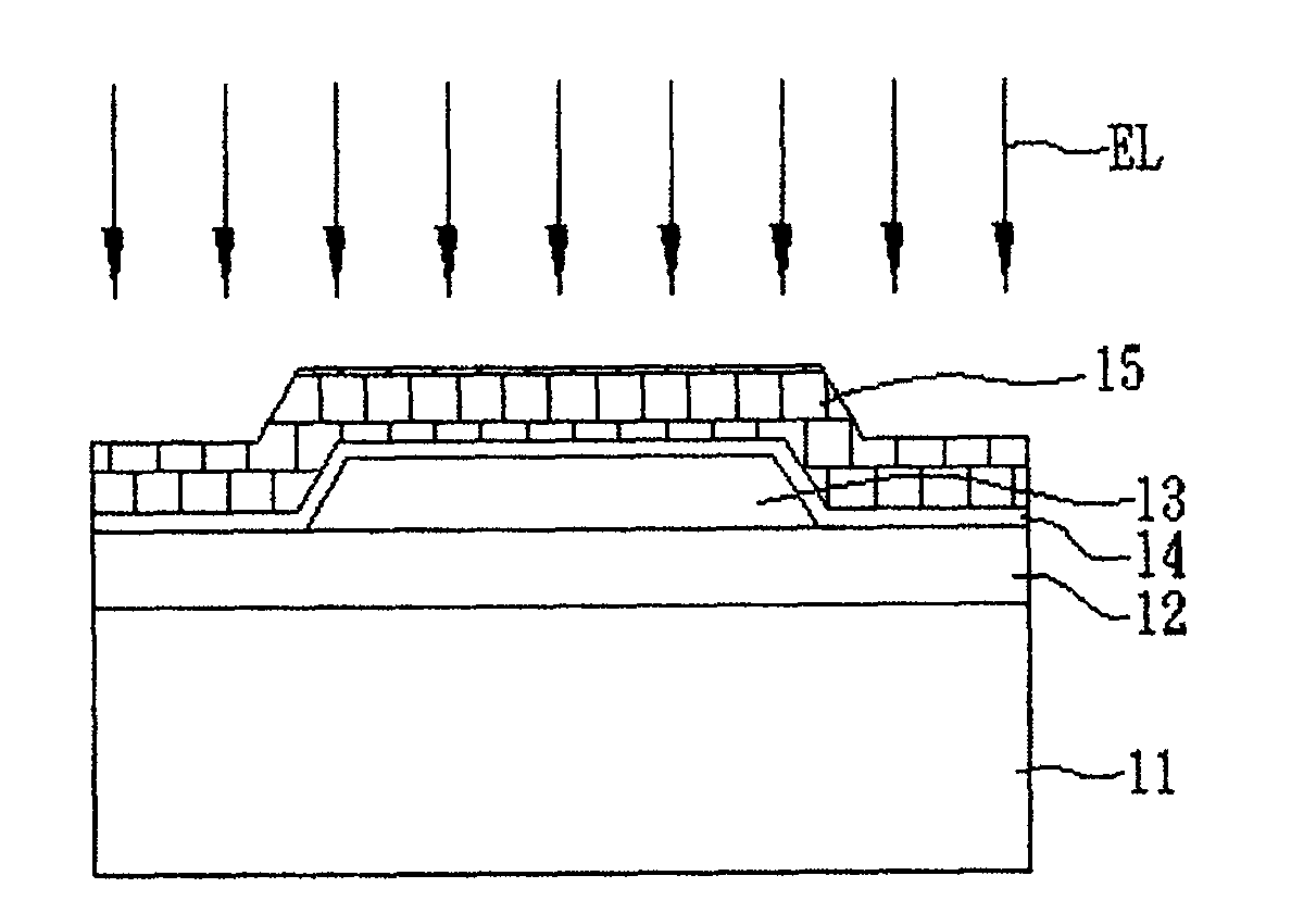
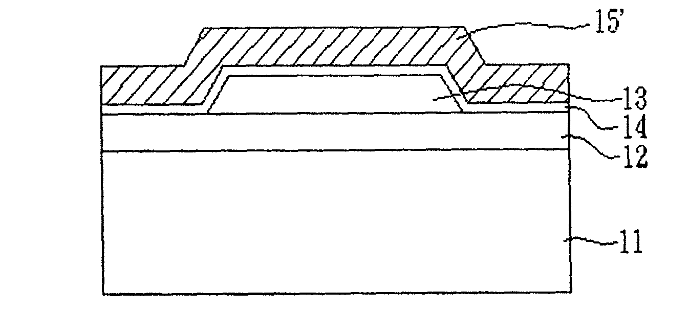
[0065] see image 3 Shown is a schematic diagram showing the structure of a low-temperature polysilicon panel according to a preferred embodiment of the present invention. A low-temperatur...


PUM


Abstract

The invention relates to a system for displaying images and a laser annealing method for low-temperature polysilicon. The low-temperature polysilicon annealing method is used for a glass substrate on which a first metal layer and a silicon film layer are formed. The annealing method includes the following steps: irradiating a laser beam with a wavelength greater than 400 nanometers on the silicon film layer, and the silicon film layer is formed on the glass substrate. The film layer absorbs a part of the laser beam and is heated and melted, and the other part of the laser beam penetrates the silicon film layer and reflects from the first metal layer to the silicon film layer, so that the silicon film layer absorbs the reflected laser beam and is reheated to crystallize ; and resting the silicon film layer after the laser beam irradiation, so that the temperature of the silicon film layer drops to room temperature. The system is used for displaying images, which includes a low-temperature polysilicon substrate with a glass substrate, a first metal layer and a polysilicon film layer. The invention can not only improve the utilization rate of the laser beam, but also save the use cost by using the solid-state laser beam, and further enhance the electron mobility of the thin film transistor.

Description

technical field [0001] The invention relates to a system and an annealing method for polysilicon, in particular to a system for displaying images that can increase the utilization rate of laser beams, save usage costs, and further improve the electron mobility of thin film transistors, and low-temperature polysilicon. Laser annealing method. Background technique [0002] With the advent of the digital age, thin film transistor liquid crystal displays have grown rapidly and become an indispensable electronic product for almost everyone or every family. [0003] Thin film transistor liquid crystal display can be divided into amorphous silicon (a-Si) thin film transistor (thin film transistor, TFT) liquid crystal display and low temperature polysilicon (low temperature polysilicon, LTPS) TFT liquid crystal display due to different liquid crystal panels, The difference between LTPSTFT display and a-Si TFT display is that LTPS TFT display uses LTPS liquid crystal panel, and LTPS...

Claims


Application Information

Patent Timeline
Patent Type & Authority Patents(China)
IPC IPC(8): H01L21/20H01L21/268H01L21/336H01L29/786H01L29/04
Inventor 森本佳宏李淂裕刘侑宗
Owner TPO DISPLAY
Why Eureka
Try Eureka