
Planar display device with pallet bottom-grid controlled structure and its production
A technology of flat panel display and bottom grid, which is applied in the direction of control electrode, discharge tube/lamp manufacturing, image/graphic display tube, etc., and can solve the problems of reducing grid operating voltage and control voltage reduction, etc.
- Summary
- Abstract
- Description
- Claims
- Application Information
AI Technical Summary
Problems solved by technology
Method used
Image

Examples
Embodiment Construction
[0038] The present invention will be further described below in conjunction with the accompanying drawings and embodiments, and the present invention is not limited to these embodiments.
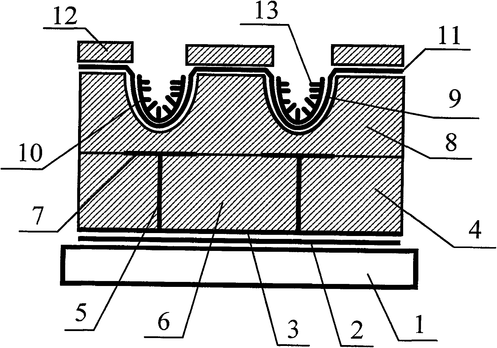
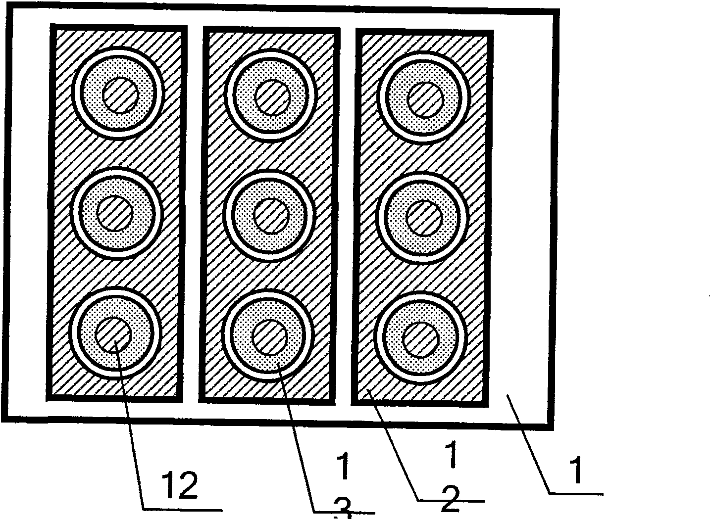
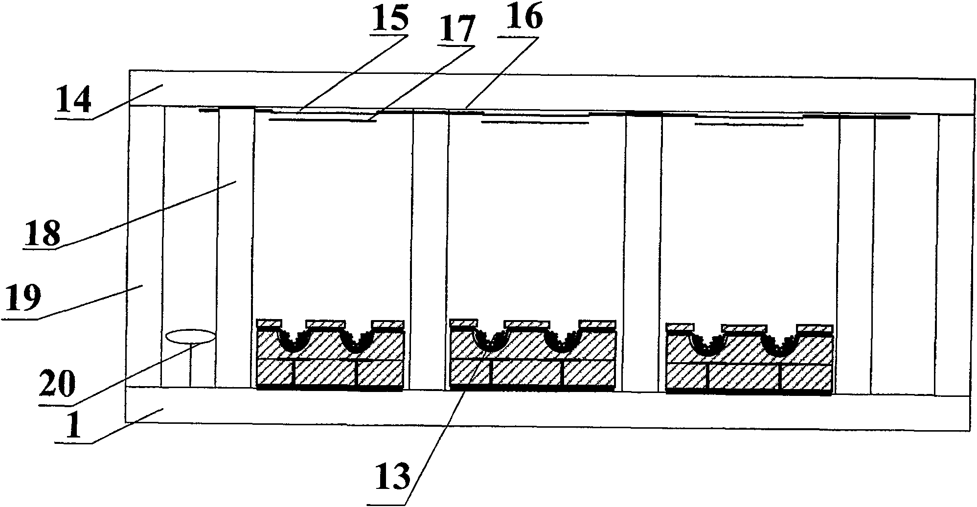
[0039] The flat panel display with a tray-type bottom grid control structure includes a sealed vacuum chamber formed by an anode glass panel [14], a cathode glass panel [1] and surrounding glass frames [19]; There is an anode conductive layer[15] and a phosphor layer[17] prepared on the anode conductive layer on the panel; there are grid lead layer[3], carbon nanotubes[13] and tray-type bottom grid control on the cathode glass panel. structure; support wall structure [18] and getter [20] accessory elements located between the anode glass panel and the cathode glass panel.
[0040] The tray-type bottom gate control structure includes a cathode glass panel [1], a retardation layer [2], a grid lead layer [3], a spacer layer [4], a grid extension line layer [5], a spacer layer layer[6], control...
PUM
 Abstract
Description
Claims
Application Information