Semiconductor storage device and manufacturing method thereof

A technology for storage devices and manufacturing methods, which is applied in semiconductor/solid-state device manufacturing, transistors, electrical components, etc., and can solve problems such as process integration of peripheral circuits of planar transistors and complex manufacturing processes of dynamic random access memory.

Active Publication Date: 2009-11-18
SEMICON MFG INT (SHANGHAI) CORP +1
View PDF4 Cites 0 Cited by
  • Summary
  • Abstract
  • Description
  • Claims
  • Application Information

AI Technical Summary

Problems solved by technology

[0004] Therefore, the object of the present invention is to provide a semiconductor storage device and its manufacturing method to solve the problem in the prior art that the gate-around transistor DRAM manufacturing process is complicated and cannot be integrated with the peripheral circuit process of the planar transistor

Method used


Image

  • Semiconductor storage device and manufacturing method thereof
  • Semiconductor storage device and manufacturing method thereof
  • Semiconductor storage device and manufacturing method thereof

Examples


Embodiment Construction

[0137] In order to make the above objects, features and advantages of the present invention more comprehensible, specific implementations of the present invention will be described in detail below in conjunction with the accompanying drawings.

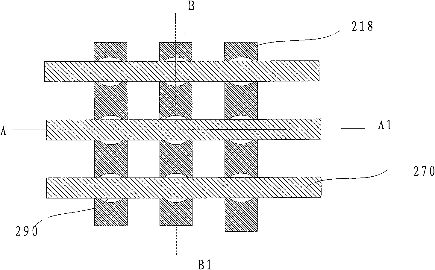
[0138] Figure 2A ~ Figure 2C It is a structural schematic diagram of the semiconductor storage device of the present invention. in Figure 2A is a top view, Figure 2B is a section cut along AA1, Figure 2C is a cut section along the direction of BB1. Such as Figure 2B or Figure 2C As shown, a conductive channel of a transistor formed by a columnar silicon island 210 is formed on the semiconductor substrate 200, and the depth of the silicon island 210 is 0.07-0.3 microns. A drain 212 is formed on the top of the silicon island 210, and an insulating layer 216 is formed on the sidewall of the silicon island 210. The insulating layer 216 may be silicon oxide (SiO2), silicon oxynitride (SiON) and other High dielectric constant ox...


PUM


Abstract

This invention discloses a semiconductor circuit and its manufacturing method, in which, said circuit includes a storage unit array and a peripheral loop, and the storage unit includes a vertical ciculating grid transistor and a groove capacitor under the transistor, the peripheral loop is composed of conventional plane transistors, the menufacturing method includes: forming a vertical circulation grid transistor array on the substrate of the semiconductor and forming a storage capacitor under the transistor.

Description

technical field [0001] The invention relates to the technical field of semiconductor manufacturing, in particular to a dynamic random access memory and a manufacturing method thereof. Background technique [0002] DRAM (Dynamic Random Access Memory) is one of the most important memory storage components at present. Due to its high function but low manufacturing cost, it is widely used in the fields of computers, communications, and home appliances. A dynamic memory cell generally includes a capacitor as a storage source for storing data and a switch and pass transistor for controlling access to data in the capacitor. In the prior art, planar transistors and stacked capacitors are mostly used. Figure 1A It is a sectional view of a dynamic random access memory unit composed of planar transistors and stacked capacitors in the prior art. Such as Figure 1A As shown, a source 101 and a drain 102 are formed on a substrate 100, and a gate structure composed of a gate oxide layer ...

Claims


Application Information

Patent Timeline
Patent Type & Authority Patents(China)
IPC IPC(8): H01L27/108H01L21/8242
Inventor 邢溯杨勇胜肖德元陈国庆
Owner SEMICON MFG INT (SHANGHAI) CORP
Why Eureka
Try Eureka