Method for eliciting sub-micron HBT emitter/HEMT grid

An emitter, sub-micron technology, applied in semiconductor/solid-state device manufacturing, semiconductor devices, electrical components, etc., can solve problems such as high etching rate, poor metal connection, and no metal exposure, so as to improve device performance and avoid Effects of poor contact and avoidance of contact

Active Publication Date: 2010-01-13
北京中科微投资管理有限责任公司
View PDF4 Cites 0 Cited by
  • Summary
  • Abstract
  • Description
  • Claims
  • Application Information

AI Technical Summary

Problems solved by technology

However, in the process of etching the dielectric planarization material, the exposed metal surface is often unclean and there are residual compounds, resulting in poor contact of the metal connection made, and at the part where the metal side is in contact with the planarization material, due to the metallization effect, The etch rate may be very high. When interconnection is made, the connecting metal may contact other circuits or devices under the metal, resulting in abnormal interconnection.
In the case of uneven planarization materials, if the etching time is not long enough, the metal in some areas will not be exposed, and the interconnection will fail to establish.

Method used


Image

  • Method for eliciting sub-micron HBT emitter/HEMT grid
  • Method for eliciting sub-micron HBT emitter/HEMT grid
  • Method for eliciting sub-micron HBT emitter/HEMT grid

Examples


Embodiment Construction

[0038] In order to make the object, technical solution and advantages of the present invention clearer, the present invention will be described in further detail below in conjunction with specific embodiments and with reference to the accompanying drawings.

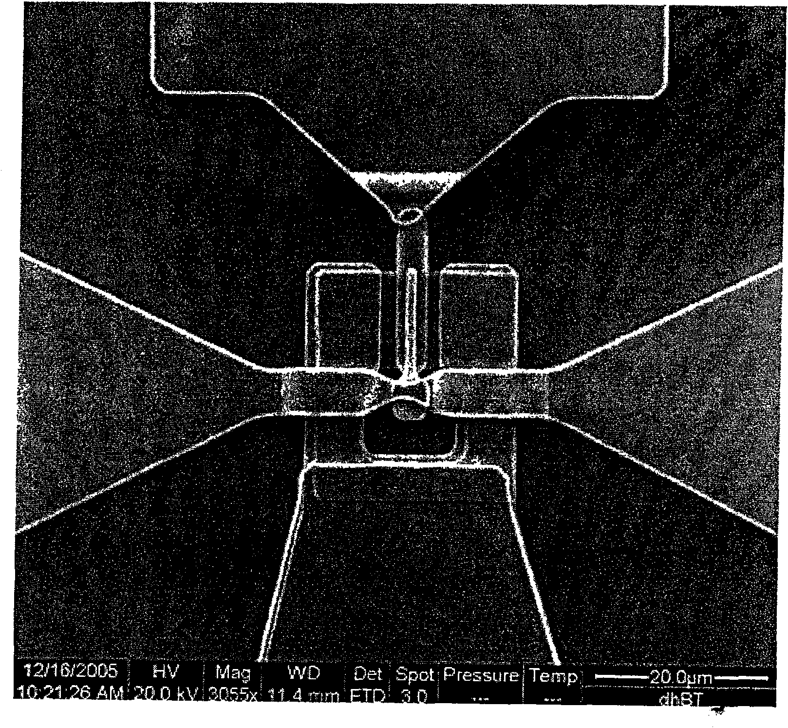
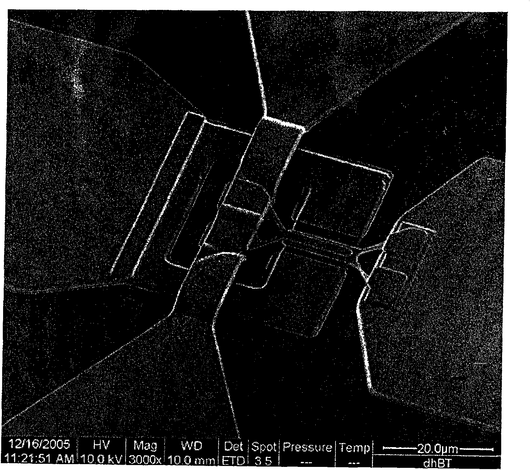
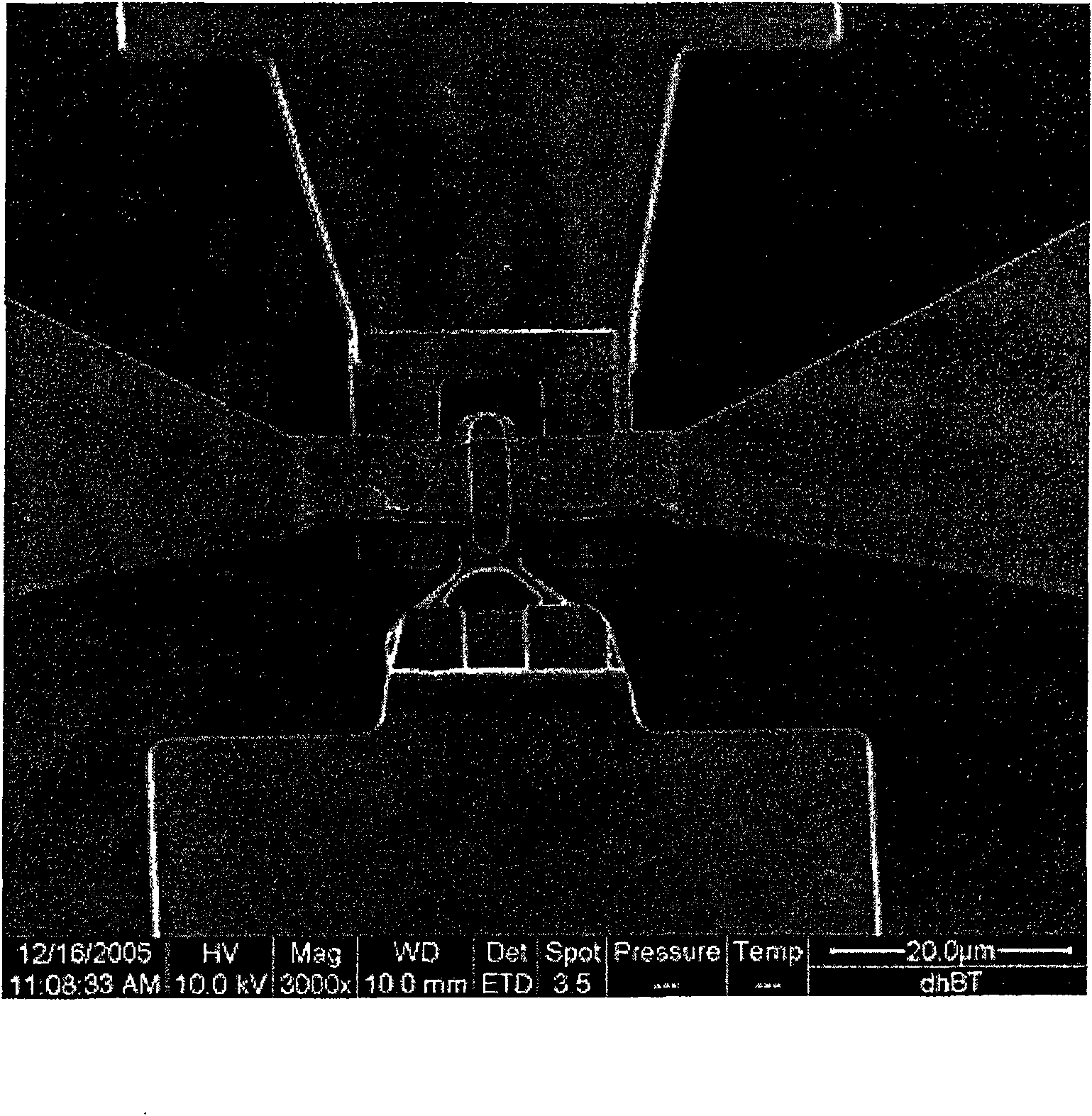
[0039] Such as Figure 4 as shown, Figure 4 It is a flowchart of a method for extracting a submicron HBT emitter / HEMT grid provided by the present invention, and the method includes the following steps:

[0040] Step 401: making a sacrificial dielectric layer on the manufactured submicron HBT emitter metal / HEMT gate metal, and peeling off to form the HBT emitter metal / HEMT gate metal with the sacrificial dielectric layer;

[0041] Step 402: coating a planarization material on the surface of the substrate having the HBT emitter / HEMT gate to make the surface of the substrate flat;

[0042] Step 403: Etching the planarization material to expose the sacrificial dielectric layer;

[0043] Step 404: removing the sacrificial...


PUM


Abstract

The invention discloses a method for eliciting sub-micron HBT emitter / HEMT grid, comprising the following steps: a sacrificial dielectric layer is manufactured on manufactured sub-micron HBT emitter metal / HEMT grid metal; the HBT emitter metal / HEMT grid metal provided with the sacrificial dielectric layer is formed by peeling; the substrate is coated with smoothing material on the surface provided with the HBT emitter / HEMT grid, so as to smooth the surface of the substrate; the smoothing material is etched and the sacrificial dielectric layer is exposed; the sacrificial dielectric layer is removed and the metal which requires interconnect is exposed; and the metal are interconnected by photo-etching and evaporating after washing. The method can be adopted to improve reliability and stability of elicitation and reduce process complexity.

Description

technical field [0001] The invention relates to the technical field of semiconductor devices and integrated circuit manufacturing, in particular to a submicron heterojunction bipolar transistor (Heterojuction Bipolar Transistor, HBT) emitter / high electron mobility transistor (High Electronic Mobility Transistor, HEMT) gate Methods. Background technique [0002] In the manufacturing process of modern semiconductor devices, with the advancement of technology, the size of the devices is getting smaller and the integration level is getting higher and higher. For compound semiconductor devices, when the submicron HBT emitter / HEMT gate is extracted, its parasitic inductance and resistance often cause a rapid decline in device performance. Therefore, the improvement of the extraction technology of the submicron HBT emitter / HEMT gate can greatly improve the performance of the device. [0003] At present, there are many ways to lead out the HBT emitter, mainly including: sub-micron...

Claims


Application Information

Patent Timeline
Patent Type & Authority Patents(China)
IPC IPC(8): H01L21/60H01L21/768
CPCH01L2924/0002
Inventor 于进勇刘新宇金智程伟夏洋
Owner 北京中科微投资管理有限责任公司
Why Eureka
Try Eureka