Method and equipment for disassembling circuit board using contacted impact

A circuit board and contact technology, which is applied in the field of circuit board disassembly and equipment using contact impact, can solve the problem of inability to disassemble inserted components, time-consuming and laborious preparation for disassembly, and poor disassembly of inserted components. question

Inactive Publication Date: 2007-08-08
TSINGHUA UNIV
View PDF8 Cites 50 Cited by
  • Summary
  • Abstract
  • Description
  • Claims
  • Application Information

AI Technical Summary

Problems solved by technology

Its disadvantages are: due to its material characteristics (the base material is mainly made of epoxy resin, glass fiber, etc. through composite methods), it becomes soft at the melting temperature of the solder, and cannot provide a uniform response to all parts of the circuit board. Elasticity; and in order to obtain sufficient resilience, the impactor bracket must push the circuit board very high, which cannot be effectively disassembled for longer plug-in components
Its disadvantages are: because the circuit board cannot be well sealed when it is installed in the device, and there are many through holes such as mounting holes and pin jacks on the substrate itself, hot air is constantly blown into the surface of the circuit board. Under normal circumstances, the lower surface of the circuit board is not easy to generate a large negative pressure, so the removal effect of the plug-in components is not good
The disadvantage is that the circuit board needs to be clamped by the clamping device to turn it over, but generally there is not enough space on the circuit board for clamping, so it is necessary to remove more components in advance, making the preparation for disassembly time-consuming and laborious. Or it needs to occupy the clamping space and damage some components; moreover, because the circuit board has softened at high temperature, the impact is implemented by rotating the impact parts, the impact force is small, and the disassembly effect on components is not good.
Its disadvantages are: the plug-in components cannot be disassembled; due to the limited heating area of ​​the strip nozzle, if the area of ​​the patch components is large, the disassembly effect will be affected; the flux that falls last will stick to the components that fell first, making Components and flux are not separated
However, using the vibration method, although larger SMD components can be disassembled, for some SMD components with small mass and volume, the disassembly effect is not good because the disassembly energy is not large enough.

Method used


Image

  • Method and equipment for disassembling circuit board using contacted impact
  • Method and equipment for disassembling circuit board using contacted impact
  • Method and equipment for disassembling circuit board using contacted impact

Examples


Embodiment 1

[0108] Example 1 According to Method 1, the circuit board with components on one side is disassembled

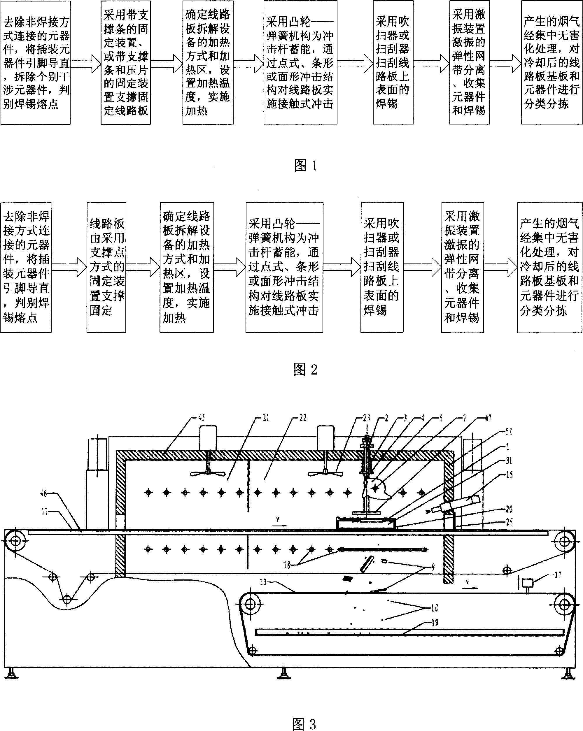
[0109] Fig. 1 is a flow chart of method 1 of the present invention. A method for dismantling a circuit board by contact impact, the method includes the following steps:

[0110] 1) Take a piece of waste circuit board with components on one side (hereinafter referred to as circuit board), such as a computer motherboard, and clean the circuit board to remove dust and dirt; Direct the pins of the plug-in components to be removed on the circuit board so that they are basically perpendicular to the circuit board substrate; roughly determine the solder (solder paste) used for the circuit board according to the type of circuit board substrate and the type of components ) melting point temperature; take the two opposite sides with the shortest distance between the opposite sides of the circuit board, and desolder and remove individual components on the circuit board, so that each s...

Embodiment 2

[0118] Example 2 According to the second method, the circuit board with components on one side is disassembled

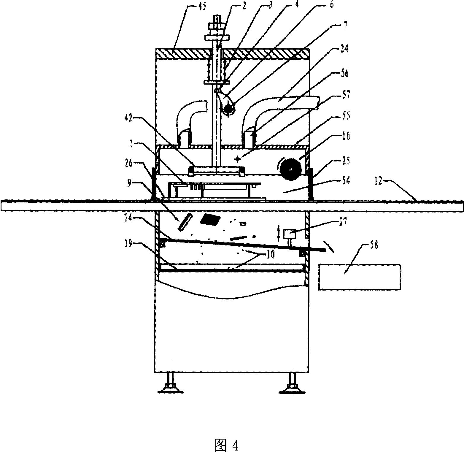
[0119] Fig. 2 is a flow chart of the second method of the present invention. A method for dismantling a circuit board by contact impact, the method includes the following steps:

[0120] 1) Take a piece of waste circuit board with components on one side (hereinafter referred to as circuit board), such as a computer motherboard, and clean the circuit board to remove dust and dirt; Direct the pins of the plug-in components to be removed on the circuit board so that they are basically perpendicular to the circuit board substrate; roughly determine the solder (solder paste) used for the circuit board according to the type of circuit board substrate and the type of components ) melting point temperature;

[0121] 2) Support the circuit board by means of support points: 4 or more adjustable support columns are arranged on a base of a grid structure; the base of the grid...

Embodiment 3

[0126] Embodiment 3 and Embodiment 4 illustrate the present invention centering on equipment.

[0127] Example 3

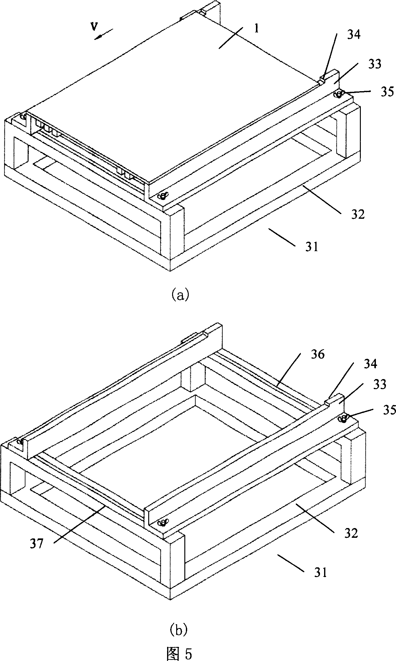
[0128] Fig. 3 is a schematic diagram of a circuit board dismantling device according to the present invention. The dismantling equipment uses support strips to fix the circuit board. The heating zone is divided into two zones: preheating zone and solder melting heating zone. It adopts multi-lift cam mechanism with gradually increasing impact energy, spring energy storage method and surface impact structure. Conduct contact impact on the circuit board with components, use the blower to purify the components and solder, and use the metal mesh belt moving horizontally to separate and collect the components and solder, so as to realize the insertion of components on the circuit board. Devices and SMD components are removed based on the integrity of their functions. This dismantling equipment can disassemble circuit boards with components on one side.

[0129] For t...


PUM


Abstract

The invention relates to one method and device to process disable by contact impact on circuit board, which comprises the following steps: fixing circuit board; heating on circuit board; adopting impact structure on circuit board for contact impact; adopting blower and collecting element parts and welding; after cooling processing the sort of circuit board and elements. The device comprises impact lever, compression spring, circuit board fix device, protruding wheel, guide rail, spring net band, and hot wind entrance hole.

Description

technical field [0001] The method and equipment for dismantling circuit boards by contact impact relate to the method and realization device for the integral and non-destructive disassembly (or removal) of components from printed circuit boards based on function recovery, belonging to production, maintenance and Waste recycling technology field. Background technique [0002] A printed circuit board (Printed Curcuit Board, referred to as PCB, or Printed Wiring Board, referred to as PWB) is an important part of electronic information products, household appliances, etc. my country is a major producer of circuit boards in the world, and tens of thousands of tons of waste circuit boards are produced in the production process every year; with the continuous upgrading of electronic and electrical products, a large number of electronic and electrical products have been eliminated, and printed circuit boards have also been abandoned. Due to the lack of proper recycling technology i...

Claims


Application Information

Patent Timeline
Patent Type & Authority Applications(China)
IPC IPC(8): H05K3/00B23K1/018B25B27/14B25B27/00
Inventor 向东汪劲松杨继平段广洪
Owner TSINGHUA UNIV
Why Eureka
Try Eureka